
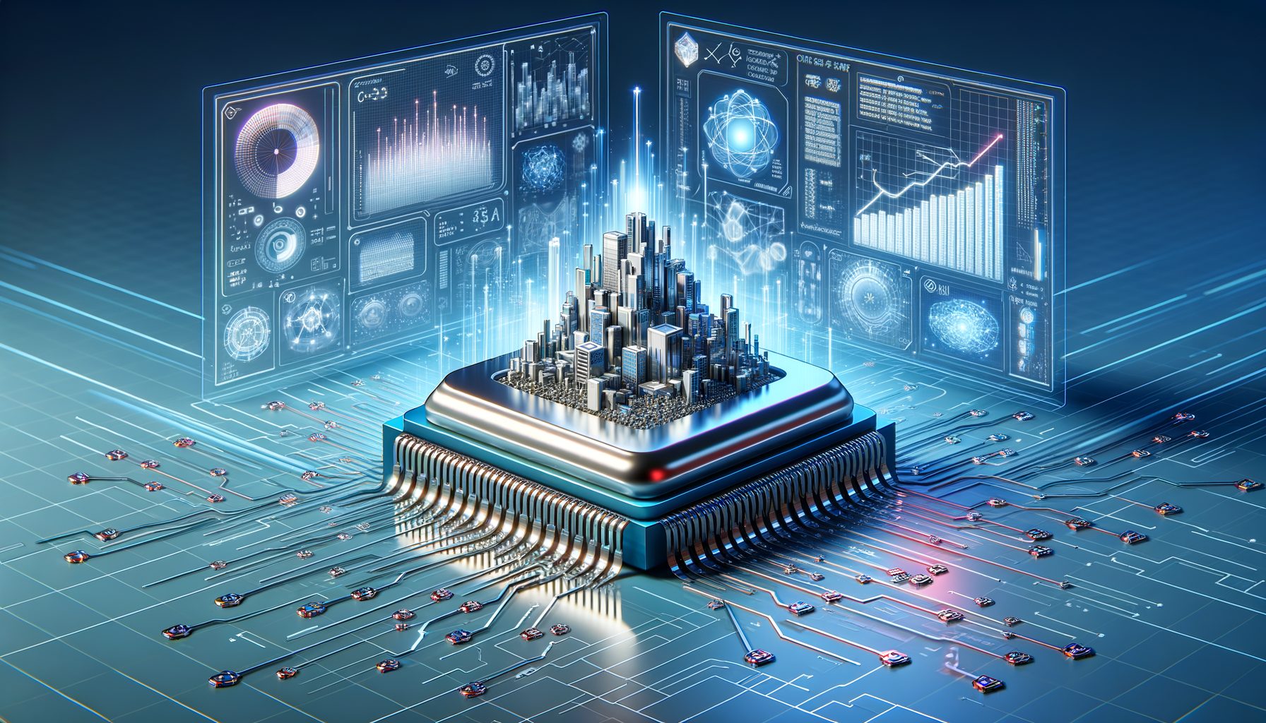
AI shows up everywhere—from photo filters and chatbots to fraud detection and drug discovery. Yet many teams still slam into slow training, pricey inference, or latency that wrecks user experience. Next‑gen AI chipsets target exactly that. By redesigning compute, memory, and power from the silicon up, they push faster, smarter machine learning without forcing a full stack rewrite. In this guide, you’ll see how these accelerators work, what’s truly new, and how to choose hardware that fits your models and budget. Curious how to go from “it works” to “it scales,” or to run sophisticated models on laptops and phones? You’re in the right place—because next‑gen AI chipsets deliver both performance and practicality.
The bottleneck: compute, memory, energy—and why next-gen AI chipsets matter
Modern AI workloads are hungry. Bigger models boost accuracy, but they multiply compute, strain memory bandwidth, and drive up energy costs. Training is only the opening act; inference at scale often becomes the bigger bill, especially for apps with millions of daily requests. Traditional CPUs weren’t built for dense linear algebra or massive parallelism. Latency creeps up. Costs spiral. Timelines stretch—right when competitive pressure says “ship faster.”
Well, here it is: three fronts where next‑gen AI chipsets hit the bottleneck head‑on.
1) Compute specialization. GPUs, TPUs, and NPUs pack thousands of smaller cores tuned for matrix math, with features like tensor cores and low‑precision arithmetic (FP8/FP4/INT8) to accelerate transformer models. 2) Memory proximity. High Bandwidth Memory (HBM) sits physically closer to compute, delivering terabytes‑per‑second bandwidth so models spend less time waiting on data. 3) Power efficiency. Better performance‑per‑watt lets you fit more usable AI into the same rack power envelope—or the battery of a laptop or phone.
Scale tells only part of the story. Users expect privacy and instant response, which pushes on‑device AI that runs without a round trip to the cloud. Meanwhile, enterprises need cloud accelerators that can crunch multi‑billion‑parameter models cost‑effectively. The edge‑versus‑cloud balance is shifting fast, and the common denominator is hardware built specifically for AI.
The shift carries real‑world impact. The International Energy Agency (IEA) estimates global data center electricity consumption could reach 620–1050 TWh by 2026, with AI as a fast‑growing contributor. Reducing energy per inference trims your bill and supports sustainability. What’s interesting too, next‑gen chipsets prioritize throughput per watt, and model optimization techniques (quantization, sparsity) are going mainstream alongside silicon advances. In short: better chips, smarter math, and tighter integration unlock the next leap in AI capability.
Inside the new architectures: GPUs, TPUs, NPUs, and the breakthroughs to watch
Accelerators aren’t all cut from the same cloth. Understanding the architectural trade‑offs helps you match the right silicon to your workload—and your deployment model.
GPUs remain the workhorse for training and large‑scale inference. Vendors like NVIDIA and AMD build tensor math into specialized cores that exploit transformer operations. NVIDIA’s latest architectures add ultra‑low precision (such as FP4) with error‑aware techniques to preserve accuracy, paired with larger HBM stacks and faster interconnects for scaling. AMD’s MI300 series uses a chiplet design to combine CPU/GPU logic and vast HBM in one package, improving memory locality and cost efficiency. Mature software stacks matter just as much: CUDA and TensorRT on NVIDIA, and ROCm with Triton kernels on AMD, help you compile and optimize models with minimal code changes. See NVIDIA’s Blackwell architecture overview and AMD’s Instinct MI300X documentation for details.
TPUs take a different route. Google’s Cloud TPU v5e and v5p are designed as data center accelerators tuned for large‑batch training and serving, tightly integrated with the XLA compiler and JAX/TF frameworks. The platform emphasizes pod‑level scaling, fast interconnect fabric, and cost‑effective throughput for production workloads. If you already run in Google Cloud or prefer high‑level graph compilation, TPUs can simplify large‑scale training pipelines.
NPUs are the rising stars on devices. Apple’s M‑series Neural Engine, Qualcomm’s Snapdragon NPUs, and similar blocks from Samsung and MediaTek optimize for power‑constrained environments with INT8/INT4 arithmetic, aggressive sparsity, and fast on‑chip memory. On‑device translation, image generation, and personal assistants become viable without a cloud call. Privacy improves, and latency stays consistent—vital for user trust and UX.
So what truly counts as “next‑gen” across these?
– Low‑precision computing made trustworthy. FP8 and FP4, combined with calibration and scaling techniques, deliver major speedups while preserving quality for many workloads.
– Memory and packaging innovations. HBM3/3E, 2.5D/3D packaging like TSMC CoWoS, and advanced chiplets bring data closer to compute, easing the “memory wall.”
– Smarter interconnects and system design. NVLink/NVSwitch, Infinity Fabric, and pod‑scale architectures cut communication bottlenecks—crucial for model parallelism and mixture‑of‑experts.
– Compiler‑led optimization. CUDA Graphs, XLA, PyTorch 2.x with TorchInductor, and vendor libraries fuse kernels, minimize memory movement, and exploit sparsity automatically.
– Then this: edge‑to‑cloud continuity. Train in the cloud, then distill or quantize for NPUs, reducing duplication and enabling hybrid inference strategies.
Bottom line: the gains aren’t about isolated speedups. They’re stacked—from math formats and kernels to packaging and networks—so the entire pipeline runs faster and cheaper.
Leading AI chipsets compared: capabilities, use cases, and ecosystem
Here’s a snapshot of widely discussed AI chipsets across cloud and edge. Specs evolve rapidly; treat it as a directional guide and follow the source links for the latest details.
| Chipset | Type | Memory | Notable metric | Best fit | Source |
|---|---|---|---|---|---|
| NVIDIA H200 / Blackwell family | GPU accelerator | Up to 141 GB HBM3e (H200); larger configs in Blackwell systems | Multi-TB/s bandwidth; FP8/FP4 support via Transformer Engine | Frontier training, high-throughput inference | NVIDIA H200, Blackwell |
| AMD Instinct MI300X | GPU accelerator | Up to 192 GB HBM3 | 5+ TB/s-class bandwidth; chiplet design | Large-context inference, cost-optimized training | AMD MI300X |
| Google Cloud TPU v5e / v5p | AI accelerator (cloud) | Pod-scale HBM; system-level capacity | Compiler-integrated scaling; cost/perf-optimized tiers | Large-scale training and serving in Google Cloud | Google Cloud TPU |
| Intel Gaudi 3 | AI accelerator | Up to 128 GB HBM (vendor specs) | High bandwidth IO; Ethernet-based scaling | Competitive training/inference with open networking | Intel Gaudi |
| Apple M4 Neural Engine | On-device NPU | Unified memory (SoC) | Up to 38 TOPS (Apple) | Local assistants, media, and creative apps on iPad/Mac | Apple M4 |
| Qualcomm Snapdragon X Elite NPU | On-device NPU (PC) | Shared LPDDR memory | Up to 45 TOPS (NPU) for on-device AI | Local copilots, creative, and productivity on laptops | Snapdragon X Elite |
How should you read this landscape?
– Cloud‑first training and heavy inference: Favor data center GPUs/accelerators with strong software ecosystems. NVIDIA’s CUDA/TensorRT stack stays the most mature for PyTorch‑first teams; AMD’s ROCm has made steady gains and is viable for many workloads. TPU is compelling if you’re aligned with Google Cloud and prefer XLA‑first pipelines using JAX/TF.
– Context‑hungry inference: Treat memory capacity and bandwidth as co‑equal with raw compute. Models with long context windows or RAG pipelines benefit from accelerators like MI300X and H200/Blackwell thanks to HBM capacity and fast interconnects.
– On‑device AI: NPUs enable private, low‑latency features without a network. For cross‑platform apps, target frameworks that compile to device NPUs (e.g., Core ML, ONNX Runtime, Qualcomm AI Stack). Quantize to INT8/INT4 and use distillation to fit tight memory and power budgets.
– Open networking vs proprietary fabrics: Ethernet‑based approaches (e.g., Gaudi) can cut vendor lock‑in and mesh with existing data center gear, while proprietary fabrics (NVLink/NVSwitch) achieve very high coupling between accelerators. Your choice shapes scaling topology and day‑to‑day operations.
Finally, look beyond peak numbers. Data loading, feature engineering, tokenization, and post‑processing can erase gains if left unoptimized. The best hardware plan comes with a matching software plan.
Choosing and deploying your AI hardware stack: practical steps that de-risk scale
Map the workload honestly before you buy or rent accelerators. Optimizing the wrong step is the fastest way to waste budget.
1) Profile first. Use PyTorch Profiler, TensorBoard, or vendor tools to pinpoint hot kernels and memory stalls. Decide whether you’re compute‑bound, memory‑bound, or IO‑bound. If tokenization or data ingestion dominates, fix that before touching silicon.
2) Start with the software. Enable mixed precision (AMP), turn on compiler backends (TorchInductor, XLA), and lean on vendor libraries (CUTLASS/cuDNN/TensorRT on NVIDIA; MIOpen/Comgr/rocBLAS on AMD). Gains of 20–50% often drop out without any hardware changes.
3) Embrace quantization and sparsity. Move from FP16 to FP8/INT8 when quality allows; calibrate with representative data and monitor accuracy drift. Where supported, structured sparsity can yield speedups. For LLMs, evaluate 4‑bit weight‑only quantization for inference to shrink memory and boost throughput.
4) Choose hardware by objective. Training giant models? Prioritize interconnect bandwidth and framework maturity. Serving LLMs with long prompts? Favor HBM capacity/bandwidth and KV‑cache optimizations. Building an AI feature for mobile or PC? Target NPUs and plan a hybrid strategy that offloads to cloud only when needed.
5) Validate with standardized benchmarks. Use MLPerf as one signal, but test your own model variants and batch sizes. Real‑world performance shifts with sequence lengths, quantization, and pre/post‑processing overhead.
6) Think in systems, not parts. Fast storage (NVMe), high‑memory CPUs for data prep, and efficient networking (200/400G) all matter. For large clusters, topology‑aware scheduling reduces cross‑node chatter and improves utilization.
7) Optimize for cost and sustainability. Spot instances, autoscaling, and right‑sized batches can slash cloud bills. On‑prem, evaluate power and cooling limits early. The IEA highlights the fast‑growing energy footprint of data centers; designing for performance‑per‑watt is fiscally and environmentally responsible.
8) De‑risk with pilots. Don’t jump to a 1,000‑GPU cluster. Run a two‑week pilot across two or three hardware options, compare TCO (including engineer time), and choose based on throughput, reliability, and ecosystem fit—not just peak TOPS or FLOPS.
9) Plan for portability. Containerize with CUDA/ROCm bases, use abstractions like ONNX Runtime or vLLM where appropriate, and keep model graphs exportable. Portability shields you from supply shocks and pricing changes.
10) Document and automate. Bake best practices into CI/CD: unit tests for numerical parity after quantization, regression checks on latency and token throughput, and energy monitoring. The fastest model is the one your team can reproduce and maintain.
Quick Q&A: common questions about next-gen AI chipsets
Q1: Do I need a GPU for every AI workload?
Not always. Small models and feature engineering can run on CPUs. For training and serving modern transformers efficiently, GPUs/accelerators shine. On‑device tasks benefit from NPUs. Match hardware to model size, latency, and budget.
Q2: What’s the difference between TOPS and FLOPS?
TOPS usually refers to integer operations (e.g., INT8) common on NPUs; FLOPS refers to floating‑point operations (e.g., FP16/FP8) used widely in training. The numbers aren’t directly comparable across formats or devices—focus on end‑to‑end latency and throughput for your workload.
Q3: How do I future‑proof my stack?
Prioritize software portability (ONNX, open compilers), keep models exportable, and avoid hard‑coding vendor‑specific ops unless necessary. Follow MLPerf, track vendor roadmaps, and design for mixed precision and quantization so new hardware features can be adopted quickly.
Q4: Are on‑device NPUs actually useful for production?
Yes. They’re great for privacy‑sensitive features, offline experiences, and instant response. Many teams go hybrid: run light tasks locally and escalate heavy prompts to the cloud.
Q5: What about memory bandwidth vs compute?
For LLM inference, memory bandwidth and capacity often gate performance due to KV‑cache access. A balanced system with ample HBM and efficient cache management can beat raw‑compute monsters that starve on memory.
Conclusion: your roadmap to faster, smarter machine learning starts now
We began with the core challenge: modern AI is constrained by compute, memory, and energy. Next‑gen AI chipsets address those bottlenecks with specialized math units, high‑bandwidth memory, and smarter packaging and interconnects. GPUs and accelerators like NVIDIA’s H200/Blackwell, AMD’s MI300X, Google’s TPU v5e/v5p, and Intel’s Gaudi 3 drive cloud‑scale training and inference. On the edge, NPUs in Apple M‑series and Qualcomm Snapdragon X Elite unlock private, low‑latency AI on devices. Across the stack, compiler advances and low‑precision formats multiply gains without sacrificing accuracy.
What should you do next? Profile your current workloads, switch on mixed precision and compilation, and measure the wins before changing hardware. Then pilot two or three accelerator options—evaluate not just peak specs, but end‑to‑end throughput, ecosystem support, and total cost. If you ship consumer features, plan a hybrid architecture: run fast, privacy‑first models on‑device and burst to the cloud only when needed. If you operate at data center scale, tune for memory bandwidth, interconnect topology, and automation. In every case, build for portability so you can pivot as supply and pricing shift.
Your competitive edge won’t come from a single chip; it will come from a system that compounds advantages—optimized models, tuned compilers, the right accelerators, and disciplined operations. Start today by benchmarking your top model with mixed precision and quantization on your current hardware, then run a short pilot on a next‑gen accelerator. The gains you measure in the next two weeks can guide the next two years of AI strategy.
AI moves fast. With the right plan, you can move faster—and smarter. Choose deliberately, test rigorously, and scale confidently. Then this: which one workload will you optimize this week to unlock momentum?
Sources and further reading
– IEA: Data centres and data transmission networks — https://www.iea.org/energy-system/buildings/data-centres-and-data-transmission-networks
– NVIDIA H200 Tensor Core GPU — https://www.nvidia.com/en-us/data-center/h200-tensor-core-gpu/
– NVIDIA Blackwell Architecture — https://www.nvidia.com/en-us/data-center/blackwell/
– AMD Instinct MI300X — https://www.amd.com/en/products/accelerators/instinct/mi300x
– Google Cloud TPU — https://cloud.google.com/tpu
– Intel Gaudi Accelerators — https://www.intel.com/content/www/us/en/products/details/accelerator/gaudi.html
– Apple M4 Neural Engine — https://www.apple.com/newsroom/2024/05/apple-unveils-breakthrough-ipad-pro-with-m4-chip/
– Qualcomm Snapdragon X Elite — https://www.qualcomm.com/products/technology/ai/products/snapdragon-x-elite
– TSMC CoWoS advanced packaging — https://www.tsmc.com/english/dedicatedFoundry/technology/CoWoS
– MLPerf benchmarks — https://mlcommons.org/en/mlperf/