
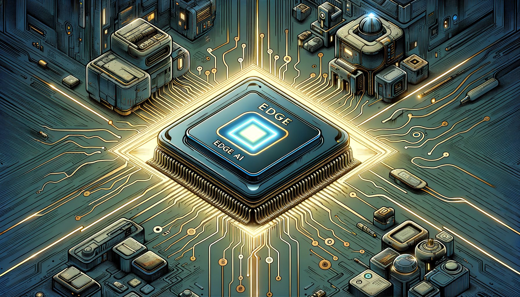
Cloud AI packs a punch, yet it can fall short on speed, privacy, and efficiency in real deployments. If a camera has to flag a hazard in a few milliseconds or a wearable must last a full day on one charge, shipping raw data to the cloud is a poor bet. By moving intelligence beside the data source, edge AI flips design assumptions and reshapes chipset roadmaps. In the pages ahead, you’ll see why edge constraints rewrite the rules, which architectures actually win, how to turn memory into the hero, and which tools and steps produce secure, updatable, production-ready on-device AI.
The new constraints of Edge AI—and why they force a different chipset strategy
Many teams hit the same wall: cloud-first instincts don’t fit edge workloads. At the edge, latency is measured in milliseconds, power budgets are counted in milliwatts, and privacy is non-negotiable. A factory robot that depends on an internet round trip to stop is unsafe. A smart speaker that uploads every utterance is hard to trust. And a battery-powered tracker that burns power on radio traffic will die before the demo is over. That’s why edge chipsets must be built for low-latency, low-power, reliable on-device inference from day one.
Such constraints flip priorities. In the data center, you chase throughput and peak TOPS; at the edge, you optimize for energy per inference, worst-case tail latency, thermal envelopes, and consistent performance under memory and bandwidth limits. Accuracy still matters, but it must be earned with quantization, sparsity, and tight memory footprints. Predictable response times are required as the environment shifts—think varying lighting for vision or different accents for speech—without cooking the device in a sealed enclosure.
One edge-specific reality stands out: the memory system dominates cost, power, and latency far more than many expect. Moving data to and from off-chip DRAM can cost orders of magnitude more energy than a multiply-accumulate operation. The game shifts from “more compute” to “better dataflow.” Architects should prioritize on-chip SRAM size and layout, efficient DMA engines, and data-reuse strategies that minimize trips to external memory. Often the right design pairs an energy-efficient neural processing unit (NPU) with a tuned memory hierarchy and a microcontroller-class CPU for control and safety.
One more truth: edge deployment is never one-and-done. Models change, regulations evolve, and security threats adapt. Secure boot, signed model updates, versioned runtimes, and telemetry hooks must be part of the chipset plan. In short, design for lifecycle—not just launch.
Architectures that win at the edge: heterogeneous SoCs, NPUs, and TinyML
No single chip fits every edge AI job, yet winners share a pattern: tightly integrated, heterogeneous compute. A typical edge SoC blends a general-purpose CPU (Arm Cortex-A/R/M or RISC‑V), a DSP for pre/post-processing, an NPU for dense linear algebra, and sometimes a GPU for graphics or parallel kernels. Such a mix lets the right engine tackle the right task: the CPU handles control and security, the DSP filters sensor data, and the NPU accelerates neural nets with low precision and high data reuse.
At the small end, microcontrollers run TinyML workloads—keyword spotting, anomaly detection, simple vision—on a few hundred kilobytes of SRAM and milliwatts of power. Frameworks like TensorFlow Lite for Microcontrollers and Apache TVM trim models to fit tight memory budgets, while vendors add MAC-friendly instructions. As shown in MLPerf Tiny results, optimized MCU pipelines can deliver real-time inference at microwatt-to-milliwatt scales, enabling always-on sensing in wearables and IoT. See the community’s benchmarks at MLPerf Tiny (MLCommons).
Move up a notch and NPUs with INT8 or even INT4 support shine on common convolutional and transformer layers. Examples include SoCs with integrated accelerators for vision and speech, as well as modules like Google Coral Edge TPU and NVIDIA Jetson Orin, which show how offloading core neural ops yields lower latency and better energy per inference than CPU-only pipelines. Not just peak TOPS, but TOPS per watt and sustained performance under thermal limits, should drive decisions.
Architectural details matter. Support for sparsity (skipping zeros) cuts compute and memory traffic. Flexible tensor cores enable mixed precision—INT8 for most layers, FP16/FP32 where accuracy demands it. Streaming architectures, where data flows linearly through compute and on-chip buffers, reduce external memory use. On the fringes, in-sensor compute and neuromorphic approaches promise further gains by processing events at the source, though software tooling and ecosystem maturity still lag. What’s interesting too: selection should start with your workload mix, target latency, and power budget—then map hardware features to those needs rather than chasing generic benchmarks.
Make memory the star: bandwidth, locality, and dataflow co-design
Ask any seasoned edge architect what breaks designs, and you’ll hear the same refrain: memory. A model that “fits” on paper can still thrash the memory system, blowing up latency and power. The fix is to design for locality. Keep weights and activations near the compute, tile work to fit on-chip SRAM, and use DMA engines to stream data predictably. With smart scheduling—conv fusion, layer reordering, double-buffering—the NPU can be kept fed while avoiding costly DRAM trips.
Why the obsession with memory? Because moving data is often more expensive than computing on it. Here’s an order-of-magnitude summary reported in academic literature; exact values vary by process and design, but the ratios tell the story clearly.
| Operation | Relative energy cost (8-bit MAC = 1x) | Notes |
|---|---|---|
| 8-bit MAC | 1x | Baseline compute cost |
| On-chip SRAM read/write | ~10–50x | Varies by width and distance on die |
| Off-chip DRAM access | ~100–1000x | Bus drivers, refresh, longer wires |
| Radio uplink (send 1 MB) | ≫1,000,000x | Dominates battery drain vs local inference |
These ratios explain why edge AI often beats cloud offload on energy and privacy: sending raw data over a network is frequently far costlier than computing locally. To exploit this, adopt a memory-first design: larger on-chip SRAM for hot tensors, wide internal interconnects for burst transfers, and compression (quantization, pruning, weight sharing) to shrink tensors. Mixed-precision INT8/INT4 can halve bandwidth needs, and structured sparsity can double effective throughput if the NPU supports it. Always evaluate on real models with representative inputs because activation sizes vary with scene complexity and sequence length.
Co-design the model as well. Replace memory-hungry layers with depthwise or grouped convolutions. Use early-exit heads when partial confidence is enough. For transformers, lean on linear attention or low-rank adapters to cut context cost. Then validate with layerwise profiling to pinpoint where the memory budget really goes. Well, here it is: if a layer does little compute per byte moved (low arithmetic intensity), move it to the DSP or fuse it to reduce bandwidth. Making memory the star turns a paper-spec chip into a real-time, reliable edge engine.
Software-first silicon: toolchains, security, and continuous optimization
Edge AI is only as good as its software. The most successful chipsets start with a software-first plan: standardized model exchange (ONNX), a robust compiler stack, and profiling tools that expose bottlenecks fast. Open toolchains like Apache TVM, vendor SDKs, and graph compilers map models onto heterogeneous hardware, handle tiling and quantization, and generate kernels that respect the memory plan you crafted. On small devices, TensorFlow Lite for Microcontrollers keeps footprints tiny and avoids dynamic allocation—critical for determinism.
Quantization-aware training, post-training calibration, and sparsity-aware pruning should be baked into your MLOps pipeline. Automate these steps so every model version arrives with measured accuracy, latency, and energy metrics. Benchmark with community suites like MLPerf Tiny and vendor datasets, and test edge cases: low light, background noise, motion blur, multi-language inputs. Focus on tail latency (p95/p99), not just averages—end users feel the slowest frames.
Security isn’t optional. Protect the boot chain with secure boot and encrypted, signed firmware. Isolate the model runtime using TrustZone or a TEE when available, and lock down debug ports before shipping. Implement A/B over-the-air updates with rollback to reduce bricking risk. Add integrity checks for model files, protect intermediate tensors if they contain PII, and log anonymized performance metrics for fleet health tracking. Then this: with these practices in place, iteration in the field becomes safe as regulations around privacy and AI transparency evolve.
Ecosystem choices matter too. Arm offers mature toolchains for AI at the edge (Arm AI at the Edge), while the RISC‑V community is rapidly standardizing vector and AI extensions (RISC‑V Technical). For model portability, ONNX keeps you flexible across vendors. Whichever path you choose, the playbook stays the same: measure, optimize, lock down, and update continuously. That’s how software turns capable silicon into a product users love.
Q&A: quick answers to common edge AI chipset questions
Q1: What is edge AI and how is it different from cloud AI?
A1: Edge AI runs models on the device where data is created—cameras, wearables, gateways—instead of sending data to the cloud. Latency drops, bandwidth is saved, privacy improves, and offline operation becomes possible. Heavy training and fleet analytics still benefit from the cloud, but when milliseconds and energy matter, inference belongs at the edge.
Q2: Do I need an NPU, or can a CPU/GPU handle it?
A2: It depends on workload and power envelope. For small always-on tasks, optimized CPU/DSP pipelines on microcontrollers work well. For mid-to-large real-time models (vision, transformer-based NLP), an NPU with INT8 support often delivers far better energy per inference and latency. Profile the model before deciding.
Q3: How do I measure success for an edge chipset?
A3: Prioritize energy per inference, p95/p99 latency, accuracy under real-world conditions, and thermal stability. Track memory footprint, resilience to noise, and OTA update reliability. Peak TOPS matters less than sustained performance within thermal and power limits.
Q4: How do I keep models secure and up to date?
A4: Use secure boot, signed and encrypted firmware/models, and A/B updates with rollback. Isolate sensitive components with TrustZone or a TEE, disable unsecured debug, and collect anonymized telemetry to guide safe updates. Build these into the chipset plan from the start.
Conclusion
Edge AI changes everything about chipset strategy. We started with the core problem: cloud-first thinking struggles with the edge’s demands for millisecond latency, tight energy budgets, and strong privacy. Next came the solution space: heterogeneous SoCs with CPUs, DSPs, and NPUs; TinyML on microcontrollers; and a memory-first approach that treats data movement as the real bottleneck. A software-first mindset—compiler tooling, quantization, continuous benchmarking—wrapped in strong security and OTA practices completes the picture. Together, these principles produce chipsets that are fast, efficient, private, and reliable in the messy real world.
Planning your next design? Define the exact workload and power envelope, profile real models with real data, and pick an architecture that maximizes locality while minimizing trips to external memory. Build the toolchain early with ONNX and a robust compiler, set up automated quantization and regression tests, and make secure updates part of the plan—not an afterthought. Use community benchmarks like MLPerf Tiny to sanity-check progress, but always validate on target scenarios. Document thermal limits, tail latency targets, and security requirements so the whole team designs to the same north star.
The future of intelligent devices belongs to teams that merge smart models with smarter silicon and the right software loop. Start small, measure honestly, iterate fast, and ship safely. Users will feel the difference in every millisecond saved and every hour of battery life gained. Ready to prototype your first edge pipeline this week and profile it on real hardware next week? The best time to begin is now—the edge waits for no one.
Build boldly. Optimize relentlessly. What will you accelerate at the edge?
Outbound resources
– MLPerf Tiny (MLCommons)
– TinyML Foundation
– ONNX model format
– Apache TVM
– Arm AI at the Edge
– RISC‑V technical resources
– Google Coral Edge TPU benchmarks
– NVIDIA Jetson Orin platform
Sources
– Horowitz, M. “1.1 Computing’s energy problem (and what we can do about it).” IEEE ISSCC 2014. Paper
– MLCommons. “MLPerf Tiny Inference.” Results and methodology
– Arm. “AI at the Edge.” Overview
– ONNX. “Open Neural Network Exchange.” Specification
– Apache TVM. “Open deep learning compiler stack.” Project