
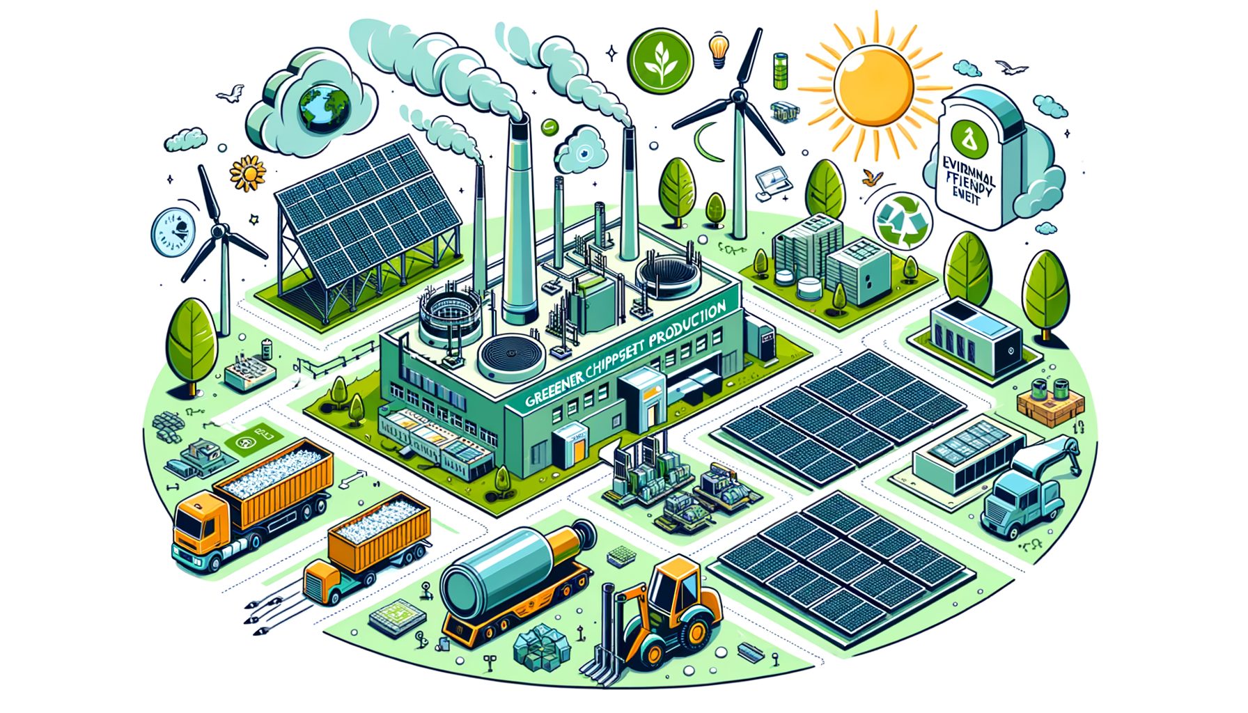
Chips power everything from climate models to your favorite mobile app. Yet the same workflows that create nanometer-scale transistors consume large amounts of energy, water, and specialty chemicals. Greener chipset production tackles that tension: crank up computing performance while dialing down environmental impact. Whether you’re a tech buyer, engineer, startup founder, or simply clean-tech curious, the guide below explains how sustainable manufacturing trends are reshaping semiconductors—and which practical steps actually move the needle.
Why Greener Chipset Production Matters Now
Modern semiconductors are built in ultra-clean factories called fabs. Complex steps—deposition, etch, lithography, polishing—run on high-purity water, substantial electricity, and fluorinated gases. The climate accounting is direct: Scope 1 covers process gases and on-site utilities; Scope 2 captures purchased electricity; Scope 3 includes upstream materials and equipment plus downstream device use. With demand soaring for AI, 5G, and electrification, total industry emissions could rise unless sustainability becomes integral. As a result, greener chipset production has shifted from “nice-to-have” to a core strategic priority for manufacturers and customers.
Three forces drive the urgency. First, policy. Regions hosting fabs—across the U.S., EU, and Asia—are tightening climate disclosure and carbon pricing. Firms that can’t trace and cut emissions face higher costs and reputational risk. Second, resilience. Water scarcity and grid constraints directly threaten uptime; conservation and on-site energy flexibility translate into continuity. Third, market pull. Cloud, consumer, and automotive leaders are setting science-based targets and demanding low-carbon products. Winning future design slots increasingly depends on credible environmental performance, not just speed and cost.
Here’s the upside: the sustainability toolkit already exists. Low-GWP chemistries, abatement systems, renewable power purchase agreements (PPAs), high-rate water recycling, smarter process control, and circular materials programs have moved from pilot to production. Even better, design choices—chiplet architectures, yield engineering—shrink footprint per compute by trimming process steps and scrap. The challenge is no longer invention but scale: adopt proven measures across fabs, nodes, and suppliers, and make sustainability an engineering requirement rather than an afterthought.
Clean Chemistry and Waste: Cutting Process Emissions at the Source
Process gases make up a sizable share of a fab’s Scope 1 emissions. Fluorinated gases like NF3, SF6, CF4, and C2F6 excel at chamber cleaning and etching, yet they carry very high global warming potentials and can persist in the atmosphere for millennia. Greener chipset production leans on three levers: substitution, reduction, and destruction.
Substitution swaps in lower-GWP gases or chemicals that achieve the same results with less climate impact. For instance, on-tool fluorine (F2) generation can replace intermediate gases with higher GWPs in some cleaning steps. In etch and deposition, shifting away from persistent perfluorocarbons (PFCs) and tuning recipes can cut emissions while preserving uniformity and throughput. Reduction depends on precision. Advanced sensors and AI-driven recipe control keep runs closer to the process window, consuming less gas per wafer and reducing rework. Cleaner runs mean less waste—and fewer emissions—from the start.
Destruction serves as the safety net. Point-of-use (POU) abatement and centralized scrubbers thermally or catalytically break down residual gases before exhaust hits the stack. Modern POU units integrate heat recovery, nitrogen reuse, and continuous monitoring to push destruction and removal efficiencies (DREs) for PFCs and NF3 to very high levels when maintained well. Maintenance is pivotal. Worn catalysts or misaligned flows can quietly underperform, so best-in-class fabs tie abatement to tool utilization data and trigger automated alerts when DRE drifts.
Waste solvents from lithography and cleaning represent another hotspot. On-site distillation and recycling can recover high-purity solvent for reuse, cutting both purchase costs and hazardous waste hauling. In chemical-mechanical planarization (CMP), life-extension tactics—slurry concentration control, pad conditioning analytics, real-time particle monitoring—reduce consumption at scale. Although trace metals and photoresist residues require careful handling, closed-loop systems with strong quality assurance can achieve circular solvent rates above 50% for selected streams in mature lines.
Standards and verification close the loop. SEMI standards such as S23 for energy, along with widely adopted environmental management frameworks, help benchmark tool performance and nudge vendors toward lower footprints. Independent measurement of gas consumption, DRE, and fugitive emissions ensures claims translate into real reductions. The bottom line: by switching chemistries, optimizing processes, and deploying robust abatement, fabs can decarbonize the hardest-to-abate emissions without sacrificing yield.
Energy, Water, and Heat: Decarbonizing Fab Utilities
Fabs run 24/7, so electricity and thermal efficiency matter. Two actions dominate impact: cut energy demand per wafer and procure clean electricity for the remainder. On the demand side, high-efficiency chillers, variable-speed drives, right-sized vacuum pumps, and heat recovery from abatement and exhaust can shave double-digit percentages from facility loads. On the supply side, long-term renewable PPAs, on-site solar where practical, and participation in demand response or energy storage programs reduce Scope 2 emissions and can stabilize operating costs.
Water sits at the center, too. Ultrapure water (UPW) rinses appear throughout wafer fabrication. Leading fabs now target UPW recycling rates above 85–90%, with some sites exceeding that for specific streams. Smart segregation—keeping lightly contaminated rinse separate from heavy-load waste—simplifies treatment and boosts recycling yield. Partnerships for indirect potable reuse with local utilities can return treated water to the community, improving regional water security. With leak detection, real-time metering, and recipe-level water coefficients, conservation becomes visible and actionable for engineers.
A lot of heat gets wasted. Integrated recovery loops can capture low-grade heat from compressors, abatement systems, and exhaust and use it to preheat UPW or for space conditioning. As boilers are electrified and high-temperature heat pumps are deployed, natural gas use can be further reduced. Combine energy and water strategies and the benefits multiply: heat recovery improves chiller performance, which cuts electricity consumption and lowers cooling tower evaporation.
Understanding gas impact helps set priorities. The table below lists 100‑year GWPs of key gases used in semiconductor manufacturing, illustrating why low-GWP substitutions and high-DRE abatement are so powerful for greener chipset production.
| Gas | Typical Use | 100-year GWP (relative to CO2 = 1) | Reference |
|---|---|---|---|
| SF6 | Chamber cleaning, dielectric etch | ~23,500 | IPCC AR6 |
| NF3 | Chamber cleaning (PECVD, CVD) | ~17,200 | IPCC AR6 |
| CF4 | Etch, cleaning | ~7,390 | IPCC AR6 |
| C2F6 | Etch, cleaning | ~12,200 | IPCC AR6 |
| CO2 | Reference gas | 1 | U.S. EPA |
For practical pathways, explore examples from technology leaders detailing renewable energy strategies, water stewardship, and facility innovation. Many publish annual ESG reports with targets and site-level progress—useful benchmarks you can adapt to your own operations.
Design, Yield, and Packaging: Shrinking the Footprint Beyond the Fab
Not all sustainability gains occur in the cleanroom. Choices made by designers, process integrators, and packaging teams can dramatically shift the footprint per unit of compute. Start with yield. Every percentage point gained cuts scrap, rework, and tool time. Statistical process control, inline metrology, and machine learning models that flag excursion risk early can lift first-pass yield without slowing cycle time. Fewer wasted steps translate into lower energy, water, and gas per good die shipped.
At the design level, chiplet architectures and advanced packaging allow large systems to be assembled from smaller dies. Yield improves because die size drops, and process intensity per delivered performance can fall. Design-technology co-optimization (DTCO) that minimizes EUV layers or consolidates steps reduces both cost and emissions. Selecting libraries and IP that are power efficient at the target workload trims downstream energy use, shrinking lifecycle footprint. Leading EDA flows now weigh power, performance, area (PPA) alongside environmental metrics, guiding layouts that balance speed with sustainability.
Packaging offers another lever. High-density substrates and 2.5D/3D integration shorten interconnects and boost system efficiency, though they add new materials and thermal constraints. Greener packaging emphasizes recycled or bio-based inputs where feasible, solvent-free adhesives, and lower-toxicity process chemistries. Thoughtful thermal design lowers junction temperatures, lengthens product life, and reduces field failures—cutting e-waste. Planning for disassembly and material recovery at design time—clear labeling, fewer mixed materials, modularity—advances circularity when devices reach end-of-life.
Supply chain sourcing matters as well. Responsible procurement of cobalt, tantalum, tin, tungsten, and gold supports human rights and reduces environmental harm in mining regions. Aligning with industry initiatives for responsible minerals and supply chain transparency builds trust and reduces risk. Wafer reclaim programs for equipment qualification, metrology wafer rental, and refurbishment of tools and parts lessen demand for new materials without compromising quality. When design, yield, and packaging teams work in concert with manufacturing, greener chipset production becomes a system-level optimization rather than a string of isolated fixes.
Practical Roadmap: How Manufacturers and Buyers Can Move Faster
Turning ambition into execution requires a clear roadmap. Begin with data. Establish a consistent carbon baseline across Scope 1, 2, and the most material Scope 3 categories. Instrument tools for granular metering and gas flow verification so engineers can link recipe choices to resource use. Adopt recognized standards and management systems to normalize reporting and make supplier collaboration easier.
Prioritize high-impact projects with short payback. Common winners include verified high-DRE POU abatement, vacuum pump right-sizing, chiller optimization, heat recovery integration, and UPW recycling expansions. Bundle these with renewable PPAs or certificates matched to your load profile to trim residual emissions. Collaborate with equipment vendors to specify lower-energy and lower-GWP options in purchase contracts, and require environmental performance data as part of factory acceptance.
Engage design and product teams early. Add sustainability gate reviews to tapeout and package selection. Incentivize yield improvements and recipe simplification by making environmental metrics visible—and by celebrating the teams that improve them. For suppliers, roll out a maturity model: bronze (basic reporting), silver (targets and pilots), gold (measurable reductions with third-party assurance). Offer technical support and share best practices so smaller suppliers can keep pace.
Finally, close the loop through transparency and collaboration. Publish progress and setbacks. Join consortia focused on sustainable semiconductors to share data and accelerate pre-competitive solutions. Encourage customers to select lower-carbon product options and co-fund decarbonization where both sides benefit. A practical roadmap blends engineering rigor with partnership—no single fab or designer can decarbonize this supply chain alone.
Q&A: Common Questions About Sustainable Semiconductor Manufacturing
Q: What makes semiconductor fabs hard to decarbonize?
A: Many process steps require high vacuum, extreme purity, and tight temperature and humidity control, which consume continuous energy. Some essential gases carry very high GWPs. The combination is complex, yet workable—chemistry substitution, abatement, efficiency, and clean power all contribute.
Q: Do advanced nodes always have a bigger footprint?
A: Advanced nodes often add steps per wafer, but they also deliver more compute per area and per watt. With strong yields and clean energy, footprint per unit performance can drop. System-level design and packaging choices are equally decisive.
Q: Are chiplets greener than monolithic dies?
A: Often yes. Smaller dies improve yield and reduce scrap, while advanced packaging can optimize performance. Net benefit depends on packaging materials, assembly yields, and how many process layers are avoided versus a single large die.
Q: How can buyers influence greener chipset production?
A: Request product-level carbon data, prefer suppliers with science-based targets, co-invest in renewable energy and abatement, and specify environmental performance in RFPs. Clear demand signals speed adoption across the supply chain.
Conclusion: From Ambition to Action in Greener Chipset Production
Greener chipset production is both responsibility and competitive edge. We covered why fabs must decarbonize now; how clean chemistry and abatement cut process emissions; how energy, water, and heat strategies decouple output from resource use; and how design, yield, and packaging decisions shrink the footprint beyond the fab. A practical roadmap emerges: measure precisely, prioritize high-impact retrofits, integrate clean power, embed sustainability into design gates, uplift suppliers, and report transparently. The thread through every step is engineering discipline—apply the same rigor used to hit nanometer tolerances to environmental goals.
Here’s your call to action. If you operate a fab, start with a targeted audit of process-gas emissions and utility hot spots, then launch a 12–18 month program bundling abatement upgrades, pump optimization, heat recovery, and UPW recycling. Sign or expand renewable PPAs to match your load. Integrate environmental metrics into tool procurement and recipe qualification. If you design chips, add carbon and water metrics to PPA dashboards, favor architectures that improve yield, and select packaging with end-of-life recovery in mind. If you’re a buyer, put lifecycle emissions into RFPs, co-fund decarbonization where it accelerates timelines, and reward suppliers who deliver verifiable reductions.
The industry has solved hard problems before—EUV, 3D NAND, chiplets. Making semiconductor manufacturing sustainable is another hard problem, yet it’s solvable when treated as a core design constraint, not an add-on. Start today with one change you can deploy within the next quarter. Then stack the wins. The chips we build will power the solutions we need—let’s build them in ways that are part of the solution, too. What’s the first move you’ll make on your greener chipset journey?
Outbound resources and further reading:
SEMI Standards (including energy and EHS)
IPCC AR6 Climate Assessment
U.S. EPA: Global Warming Potentials
imec: Sustainable Semiconductor Technologies & Assessment
Intel: Global Water Stewardship
Samsung: Environmental Sustainability
Responsible Business Alliance
Responsible Minerals Initiative
Sources:
• Intergovernmental Panel on Climate Change (IPCC) AR6 Reports: https://www.ipcc.ch/assessment-report/ar6/
• U.S. Environmental Protection Agency (EPA) Global Warming Potentials: https://www.epa.gov/ghgemissions/understanding-global-warming-potentials
• SEMI Standards Overview: https://www.semi.org/en/resources/standards
• imec Sustainable Semiconductor Research: https://www.imec-int.com/en/research/sustainable-semiconductor-technologies-systems-assesment-susta
• Intel Water Stewardship Programs: https://www.intel.com/content/www/us/en/corporate-responsibility/global-water-stewardship.html
• Samsung Environmental Initiatives: https://www.samsung.com/global/sustainability/environment/
• Responsible Business Alliance (RBA): https://www.responsiblebusiness.org/
• Responsible Minerals Initiative (RMI): https://www.responsiblemineralsinitiative.org/