
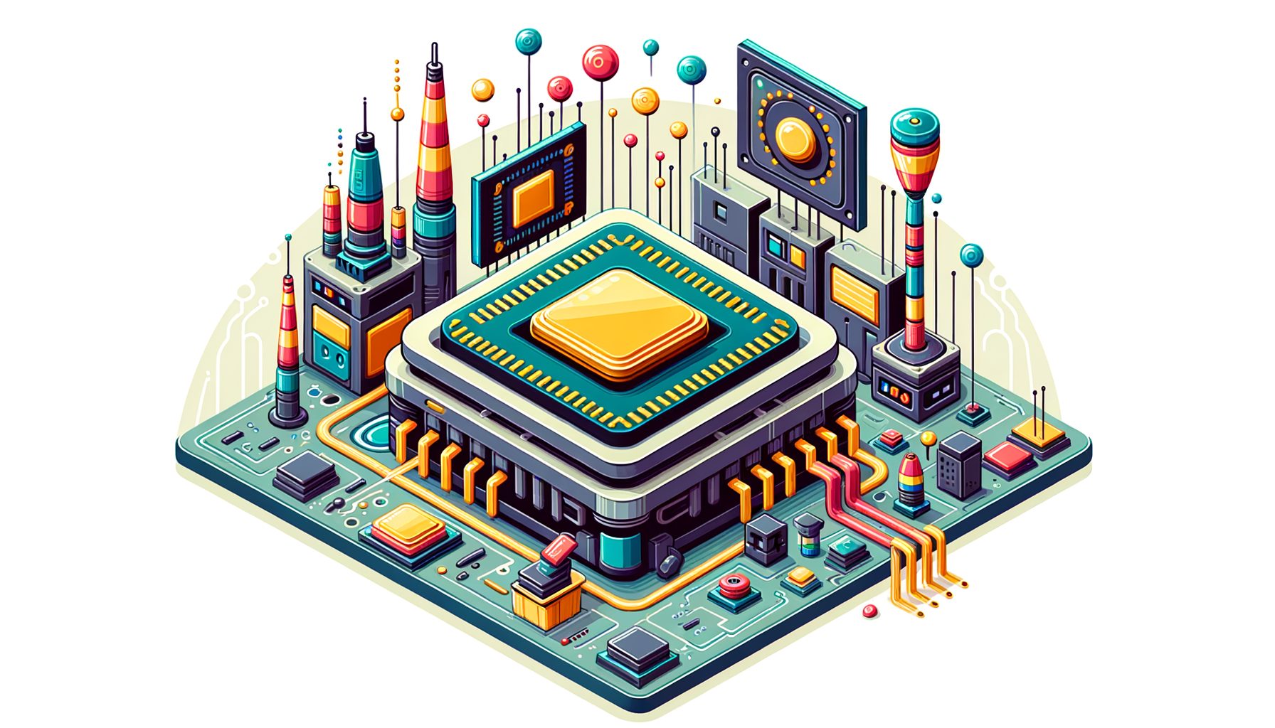
Monolithic chips are running into hard limits: costs are soaring at advanced nodes, defect rates punish large dies, and power/thermal budgets cap performance. That’s where chiplet technology steps in. By splitting a processor into smaller, specialized dies connected through ultra-fast links, engineers can build bigger, more capable systems without making a single giant, fragile die. If you’ve heard about modular design in semiconductors and wondered how it really changes CPUs, GPUs, and AI accelerators, consider this your tour with clear examples, concrete benefits, and practical considerations.
The problem chiplets solve: scaling beyond monolithic processors
For decades, the industry scaled performance by shrinking transistors and packing more of them into a single die. But as we push into advanced process nodes, that old approach faces three stubborn obstacles. First, costs. The latest nodes are astronomically expensive, and yield—the percentage of good dies per wafer—drops rapidly as die size grows. One minor defect can ruin a large, expensive chip. Second, physics. Power density and heat make it increasingly difficult to raise frequencies or add more cores without throttling. Third, manufacturing limits. Lithography tools impose a “reticle limit,” roughly the maximum area a single die can occupy; this caps how big a monolithic chip can be before it must be split or stitched, which gets complex and costly.
Chiplets address these realities head-on. Instead of one giant die, designers create several smaller dies—compute, I/O, memory cache, or accelerators—and link them together. Because smaller dies have higher yield, total cost per functional processor can fall even when the full package is more complex. Plus, each chiplet can be manufactured on the most suitable process: cutting-edge nodes for compute cores, mature nodes for analog or I/O, and potentially different foundries for different functions. Such heterogeneous integration delivers flexibility that a single-die approach can’t match.
Real-world results already validate this shift. Server CPUs built with chiplets pack dozens of cores, huge caches, and high memory bandwidth, yet they remain economically viable thanks to yield gains from smaller compute tiles. Meanwhile, laptop processors are emerging with separate tiles for CPU, GPU, NPU, and I/O integrated using advanced packaging. Across cloud servers, gaming rigs, and AI systems, chiplets make it feasible to scale performance without betting everything on one massive die.
There’s also a time-to-market advantage. Teams can iterate on one tile (say, a new NPU) without redesigning the entire SoC, speeding innovation. In a world where AI and software stacks evolve monthly, that agility matters as much as raw performance.
How chiplet architecture works: modular design, packaging, and die-to-die links
At a high level, a chiplet-based processor is a small network of specialized dies stitched together with short-reach, high-bandwidth interconnects inside one package. A typical design might include: compute chiplets (CPU cores or GPU compute units), an I/O or base die that handles memory controllers and external interfaces, and optional accelerator chiplets for AI or media. The “secret sauce” is the die-to-die fabric that makes multiple dies behave as one coherent system with minimal overhead.
Two enablers make this possible. First, advanced packaging: instead of mounting a single die on an organic substrate, vendors use 2.5D silicon interposers, silicon bridges, or 3D stacking. These techniques shorten wire lengths dramatically and raise bandwidth per millimeter while cutting latency and power per bit moved. Second, standardized interfaces: the Universal Chiplet Interconnect Express (UCIe) initiative defines a common, open die-to-die interface that supports high bandwidth density and low latency, aiming to let chiplets from different vendors interoperate in the future. While early products still use proprietary links, the industry trend points toward more open, ecosystem-friendly connectivity.
Choosing the right packaging depends on performance targets, thermals, and cost. Organic substrates are cheaper and simpler but have lower bandwidth density. Silicon interposers (like TSMC CoWoS) and silicon bridges (like Intel EMIB) provide more routing density and signal integrity. 3D stacking (Intel Foveros, TSMC SoIC) goes vertical: logic-on-logic or cache-on-logic stacking can slash wire length and deliver massive bandwidth with excellent energy efficiency, albeit with tighter thermal and manufacturing constraints.
Here’s a quick comparative look at common approaches. Values are relative because exact numbers vary by node, pitch, process, and implementation.
| Packaging approach | Typical use | Bandwidth density | Power per bit | Relative cost/complexity |
|---|---|---|---|---|
| Organic substrate (MCM) | Cost-optimized multi-die CPUs/SoCs | Low to medium | Higher | Low |
| 2.5D silicon interposer (e.g., CoWoS) | High-bandwidth CPU/GPU with HBM | High | Medium to low | Medium to high |
| Silicon bridge (e.g., EMIB) | Localized high-speed chiplet links | Medium to high | Medium | Medium |
| 3D stacking (Foveros, SoIC) | Logic-on-logic, cache-on-logic | Very high | Low | High |
On the design side, engineers partition functionality to minimize chatty cross-die traffic and place latency-sensitive blocks close together (physically and logically). They model bandwidth needs, thermal paths, and power delivery early, then co-optimize chiplets with the package. Verification spans dies, package, and firmware: a chiplet system only feels “monolithic” to software if the hardware fabric is fast, reliable, and well-abstracted. That’s exactly what modern die-to-die protocols and packaging aim to deliver.
Benefits and trade-offs: performance per watt, cost, flexibility, and risks
The headline benefit is scalable performance per watt. Short interconnects and dense routing within the package provide far higher bandwidth at lower energy per bit than board-level links. That’s critical for AI-era workloads that move terabytes per second between compute and memory. Combining chiplets also helps designers keep hot logic on leading-edge nodes while offloading analog, I/O, or large SRAM to nodes with better leakage, cost, or device options. The result is often better performance at lower power and lower total cost than an equivalent monolithic die.
Another major upside is yield and cost control. Yield typically drops as die area increases, so using several small chiplets can sharply raise the number of usable parts per wafer. Public analyses of multi-chip server CPUs have shown substantial cost reductions by trading one giant die for multiple smaller compute tiles plus an I/O die. The economics become even more favorable as defect densities at advanced nodes fluctuate—smaller chiplets absorb those shocks better, keeping supply more predictable.
Flexibility is a quiet superpower. Teams can mix-and-match: integrate a new AI accelerator chiplet this year without re-spinning the I/O tile; ship a cloud version with extra memory bandwidth and an edge version with a beefier NPU; or swap foundries for one tile while keeping the rest unchanged. Such agility shortens product cycles and reduces risk.
But trade-offs are real. First, integration complexity: partitioning, packaging, signal integrity, power delivery, and thermal paths all get harder. Second, latency and coherency: not all links are equal, and poorly planned fabrics can bottleneck chatty workloads. Third, thermals: stacking and tight die placement can create hotspots that require advanced materials and cooling. Fourth, verification and security: multi-die validation spans more failure modes; on-package interfaces need protection against fault injection or side channels just like off-package links.
Finally, supply chain orchestration becomes strategic. Sourcing multiple dies, potentially from different geometries or vendors, demands tight collaboration, IP licensing clarity, and robust test strategies (known-good-die is a must). Despite the challenges, the upside—in performance, cost, sustainability, and speed of innovation—makes chiplets the default path forward for many categories of processors.
Real-world examples and what’s next: CPUs, GPUs, and AI accelerators
Chiplets aren’t theoretical—they’re already powering headline systems. In servers, multi-tile CPUs deliver high core counts and broad memory I/O by pairing compute chiplets with a central I/O die. The approach has scaled across several generations, proving that the performance and economic gains persist even as core counts climb. On the client side, hybrid laptop processors now use separate CPU, graphics, and media/AI tiles stacked or bridged with advanced packaging, improving efficiency and letting vendors update subsystems independently.
GPUs and AI accelerators are following suit. Modern high-performance GPU packages integrate logic dies with stacks of High Bandwidth Memory (HBM) on silicon interposers, pushing enormous throughput for training and inference while keeping energy per bit low. As GPU architectures evolve, expect more explicit multi-die splits, with dedicated chiplets for compute, cache, and I/O stitched via silicon bridges or interposers. That kind of modular design matches the heavy, bursty data flows in AI and graphics and eases scaling across product tiers.
Perhaps the most transformative change is standardization. The UCIe Consortium is working toward a shared interconnect so chiplets can interoperate beyond single-vendor ecosystems. Today, most products still use proprietary links optimized for their architecture. But as UCIe matures and packaging roadmaps stabilize, we’ll see broader marketplaces of reusable chiplets: think of it as a “component store” for silicon, where verified tiles for compute, security, memory, or RF can be composed into an SoC faster than before.
Advanced packaging tech is accelerating in parallel. 2.5D interposers (TSMC CoWoS), silicon bridges (Intel EMIB), and 3D stacking (Intel Foveros, TSMC SoIC) are increasing bandwidth density and reducing energy per bit each generation. The industry is also scaling the supply of larger interposers and more HBM stacks to feed AI demand. That infrastructure growth matters: packaging capacity and yield are now as strategic as wafer capacity at the leading nodes.
Looking ahead, expect three clear trends. First, heterogeneous integration will extend beyond CPU+GPU to include dedicated NPUs, memory-centric accelerators, and domain-specific tiles. Second, security and reliability features will move into the die-to-die fabric—measured boot across tiles, encrypted links, and standardized RAS (reliability, availability, serviceability). Third, sustainability will matter more: better yields from smaller chiplets and the ability to reuse base dies across product cycles can reduce waste and improve lifecycle footprints.
Practical guide: what to evaluate if you build or buy chiplet-based systems
If you’re an engineer planning a chiplet design, start with partitioning. Identify which blocks truly need bleeding-edge nodes (e.g., vector compute) and which can sit on mature nodes (e.g., PHYs, SRAM-heavy cache, analog). Model cross-die traffic early: co-locate chatty blocks on the same die or connect them with the fastest link available. Define performance budgets in bandwidth (GB/s), latency (ns), and energy per bit (pJ/bit), and map those to packaging choices. Then co-design with your packaging house: power delivery networks, thermal interfaces, and mechanical constraints (warpage, CTE mismatches) must be solved alongside logic design, not after the fact. Finally, invest in system-level verification across dies and package, including stress tests for coherency, link margining, and thermal throttling behaviors.
For buyers—CIOs, IT leads, enthusiasts—compare chiplet systems with a few key questions. What is the die-to-die link bandwidth and latency, and how does it scale across SKUs? Is memory coherency maintained across chiplets, and what’s the penalty under mixed workloads? How is thermal density handled—are there vapor chambers, 3D TIMs, or stacked-die guards? What is the vendor’s test strategy (known-good-die, built-in link diagnostics)? On the software side, check whether the OS, drivers, and compilers are aware of chiplet topology to place threads, memory, and accelerator tasks intelligently.
Look for transparent specs. Leading vendors publish package diagrams, bandwidth figures, and supported standards. If the product relies on advanced packaging like 2.5D interposers or 3D stacking, ensure the supply chain can keep up with demand—packaging capacity has become a real constraint for AI-class devices. Also evaluate longevity: can you expect compatible upgrades where new chiplets (e.g., an updated accelerator tile) drop into the same platform, extending lifecycle value?
Security and reliability deserve a spotlight. Ask whether die-to-die links support encryption or integrity checks, and how fault isolation works if one tile misbehaves. For mission-critical deployments, look for documented RAS features and root-cause tools that can differentiate between die, link, and package issues. Finally, consider sustainability: multi-die designs can improve yields and cut scrap, and modularity may enable partial refreshes instead of full rip-and-replace systems.
Bottom line: whether you’re building or buying, treat chiplet architecture as a system design problem. The best outcomes come from balancing compute, memory, fabric, thermals, and software together—and choosing vendors who share real data, not just marketing claims.
Q&A: common questions about chiplet technology
Q: Is a chiplet-based processor slower than a single big chip? A: Not inherently. When designed well, chiplet systems deliver equal or better performance because they use fast, short-reach on-package links with high bandwidth density. Latency can be slightly higher than on-die for cross-chiplet traffic, but smart partitioning keeps most hot data local. In practice, the performance per watt often improves thanks to better node choices and shorter interconnects than board-level designs.
Q: Why do chiplets reduce cost if the package is more complex? A: Smaller dies have higher yield, which means more usable parts per wafer. Even after paying for advanced packaging, the total cost per working processor can drop compared to one giant die that loses yield to defects. The effect becomes more pronounced at advanced nodes where wafer costs are high and defects are costly.
Q: Can different companies’ chiplets work together? A: That’s the vision behind UCIe (Universal Chiplet Interconnect Express). Today, most products still rely on vendor-specific links optimized for their architecture. As UCIe and related standards mature, you can expect more multi-vendor interoperability, though certification, security, and IP licensing will remain important practical considerations.
Q: What about thermals—won’t stacking make hotspots worse? A: Thermal design is a major focus. Vendors use careful die placement, heat spreaders, vapor chambers, and advanced TIMs to manage heat. 3D stacking does increase thermal density, but it also shortens interconnects, which cuts I/O power. With proper co-design of package, cooling, and power delivery, stacked and bridged designs meet or exceed traditional thermal limits.
Q: How does this help AI workloads specifically? A: AI training and inference move vast amounts of data between memory and compute. On-package links (and HBM on interposers) provide much higher bandwidth at lower energy than off-package alternatives. Modular designs can also add dedicated AI accelerators (NPUs) alongside CPUs/GPUs, scaling up or down for cloud and edge. The result is better throughput, efficiency, and flexibility as models and software evolve.
Conclusion
Across modern computing—from cloud servers to laptops to AI accelerators—modularity is winning. Chiplets turn a single, hard-to-build mega-die into a well-orchestrated team of smaller, specialized dies connected by fast, efficient on-package links. That shift solves real problems: it eases manufacturing limits, reduces cost through higher yield, and lets designers pick the right process for each function. It also adds agility at a time when workloads and software stacks change faster than traditional SoC cycles.
In this article, we explored why monolithic scaling is stalling, how chiplet architectures work, and what advanced packaging and standards like UCIe bring to the table. We looked at the benefits—performance per watt, flexibility, sustainability—and the trade-offs around integration, coherency, thermals, and supply chain orchestration. We highlighted real products and offered a practical checklist for builders and buyers to evaluate chiplet-based systems with confidence.
If you’re planning a roadmap, now is the moment to pilot modular designs: benchmark die-to-die fabrics, evaluate packaging partners, and model cross-die traffic for your workload mix. If you’re buying, insist on transparent specifications—bandwidth, latency, thermal solutions, RAS features—and prioritize vendors who show their work with credible data. Either way, start the conversation today: the ideas you test this quarter become your competitive edge next year.
Tomorrow’s performance gains won’t come from brute force alone; they’ll come from smart composition. Take the next step—download a vendor white paper, compare a chiplet-based SKU to your current platform, or set up a small proof-of-concept. The future of processors is modular, and it’s arriving faster than you think. What will you build with it?
Useful links for deeper exploration:
UCIe Consortium (Universal Chiplet Interconnect Express)
AMD Zen core and multi-chip design overview
Intel advanced packaging (Foveros, EMIB)
TSMC advanced packaging (CoWoS, InFO, SoIC)
IEEE Spectrum coverage on chiplets
Sources:
UCIe 1.0/1.1 specifications and FAQs: https://www.uciexpress.org
AMD multi-die CPU architecture insights (Zen generations): https://www.amd.com/en/corporate/technology/zen-core
Intel Foveros and EMIB technology briefs: https://www.intel.com/content/www/us/en/newsroom/resources/advanced-packaging.html
TSMC CoWoS/InFO/SoIC overview: https://www.tsmc.com/english/dedicatedFoundry/technology/advanced-packaging
IEEE Spectrum on chiplet trends and ecosystem: https://spectrum.ieee.org/chiplets