
If you’ve ever compared two laptops or phones that look similar on paper but perform very differently, you’ve already felt the hidden power of Chipset Architecture. Behind the scenes, the design routes data between your CPU, memory, storage, graphics, and every port you plug into. Get it right, and everything feels instant. Get it wrong, and you’ll notice slow file transfers, game stutter, battery drain, or thermal throttling. Here’s a practical starter guide that demystifies Chipset Architecture, traces how it evolved, and gives you steps to pick the right device while avoiding real‑world bottlenecks.
Why Chipset Architecture Matters: The Basics and Terminology
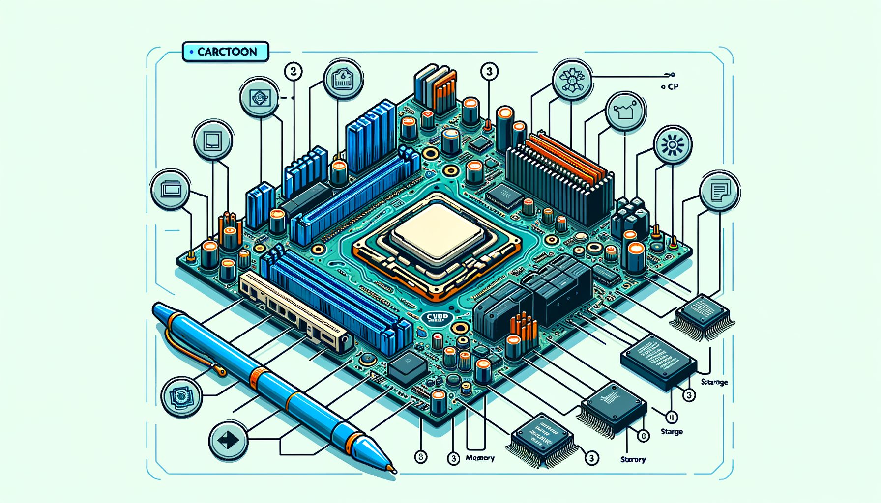
At a high level, a chipset is the connective tissue of a computer or phone. In desktops and many laptops, the CPU handles the heavy math and some memory tasks, while a Platform Controller Hub (PCH) or I/O controller manages connectivity like USB, SATA, Wi‑Fi, and sometimes PCI Express lanes. Smartphones—and many modern laptops—use a System on a Chip (SoC) that integrates CPU, GPU, memory controller, neural engines, and I/O into a single package. Design choices in Chipset Architecture set the ceiling for bandwidth (how much data can move), latency (how quickly a response comes), power efficiency, and expandability.
Three terms to lock in: memory controller, I/O fabric, and lanes. The memory controller decides how quickly the CPU and GPU access RAM. The I/O fabric acts as the internal highway that connects controllers to each other and to the CPU. Lanes (often PCIe lanes on PCs) are the point‑to‑point links that devices use to talk at high speed. Fewer lanes or older standards can cap performance even if individual parts look fast. For example, a powerful NVMe SSD can be limited by a slot that shares lanes with Wi‑Fi or SATA, or by being wired for PCIe Gen 3 instead of Gen 4/5.
In practice, balanced Chipset Architecture feels like this: your game streams textures smoothly because the GPU has a full‑bandwidth link and the SSD gets its own dedicated lanes; 4K video exports run faster because the CPU, GPU, and media engines can all reach RAM at high speed; your phone launches apps instantly because the SoC’s memory controller, storage (UFS/NVMe), and neural cores are tightly integrated. When the architecture is unbalanced, symptoms show up as USB ports slowing down under load, M.2 drives dropping speed when other ports are used, or Wi‑Fi performance tanking when a webcam is plugged in.
For deeper official definitions and components, see Intel’s overview of platform controller hubs at intel.com and ARM’s SoC architecture resources at developer.arm.com.
Evolution: From Northbridge and Southbridge to SoC and Chiplets
Early PC motherboards used a two‑chip design: the northbridge handled high‑speed tasks like memory and the graphics link, while the southbridge managed lower‑speed I/O such as USB and SATA. Around the late 2000s, CPU makers integrated the memory controller (and often graphics) into the processor itself. That change removed the northbridge, cut latency, and increased memory bandwidth. Remaining functions moved into a single PCH connected to the CPU via a fast link (e.g., Intel DMI or AMD’s equivalent), which simplified boards and improved power efficiency.
Phones embraced the System on a Chip (SoC) model from the start. A modern SoC merges CPU cores, GPU, image signal processors, media encoders/decoders, AI accelerators, and the memory controller on the same piece of silicon. Such tight integration delivers huge efficiency gains—vital for battery life—while enabling features like 8K video capture or on‑device AI without round‑trips across slower buses. Apple’s M‑series and many Windows‑on‑ARM laptops brought the SoC approach to personal computers, with unified memory and shared fabric that help graphics and AI tasks move data faster and consume less power.
Then this: chiplets (or tiles) changed how processors are built. Instead of one giant chip, manufacturers create multiple smaller dies—each optimized for a job like CPU cores, I/O, cache, or GPU—and link them with high‑speed interconnects. AMD’s Ryzen and EPYC processors popularized the approach via Infinity Fabric, while Intel uses techniques like EMIB and Foveros stacking to connect tiles. An emerging open standard, UCIe (Universal Chiplet Interconnect Express), aims to let chiplets from different vendors talk over common links. The benefits include better yields, modular upgrades, and the ability to mix cutting‑edge and mature manufacturing nodes in one package. For readers, that means more performance and features per watt, with a chance for faster innovation cycles. Explore these directions at amd.com, intel.com, and the UCIe consortium at uciexpress.org.
Performance in Practice: Buses, Lanes, and Bottlenecks You Can Avoid
Bandwidth numbers are the most visible part of Chipset Architecture. They tell you how fast data can move—if the device, slot, and chipset all align. Well, here it is: typical, rounded figures to anchor expectations when you shop or troubleshoot.
| Interface | Typical version | Approx. max bandwidth | What it means in real life |
|---|---|---|---|
| PCIe 3.0 x4 (NVMe) | Gen 3 | ~3.9 GB/s | Good for most SSDs; can limit top‑tier drives |
| PCIe 4.0 x4 (NVMe) | Gen 4 | ~7.9 GB/s | Common on modern desktops/laptops; ideal for fast storage |
| PCIe 5.0 x4 (NVMe) | Gen 5 | ~15.8 GB/s | Next‑gen SSDs; watch thermals and lane sharing |
| USB 3.2 Gen 2 | 10 Gbps | ~1.2 GB/s | Fast external SSDs; shared hubs can reduce speed |
| USB4 / Thunderbolt 4 | 40 Gbps | ~5 GB/s | High‑end docks, eGPUs; performance depends on PCIe tunneling |
| SATA III | 6 Gbps | ~0.6 GB/s | Fine for HDDs and many 2.5″ SSDs |
| LPDDR5 @ 6400 MT/s (64‑bit) | Mobile RAM | ~51.2 GB/s | Unified memory on SoCs boosts GPU/AI throughput |
| Wi‑Fi 6E (2×2, 160 MHz) | AX | ~2.4 Gbps | About 300 MB/s ideal; real speeds vary with signal |
Numbers are theoretical maxima; protocol overhead, device firmware, and thermal limits reduce real‑world throughput. Always cross‑check device and motherboard manuals. See standards and specs from PCI‑SIG (pcisig.com), USB‑IF (usb.org), and JEDEC (jedec.org).
Practical steps to avoid bottlenecks:
1) Map your lanes. On PCs, the CPU usually provides a primary PCIe slot and one or more NVMe connections, while the chipset/PCH adds extra lanes for more NVMe, SATA, and USB. Some M.2 slots share lanes with SATA ports; using one can disable the other. Motherboard block diagrams often reveal this. For storage‑heavy setups, prioritize CPU‑direct NVMe slots for your fastest SSD.
2) Match standards intentionally. A PCIe 4.0 SSD in a PCIe 3.0 slot will still work but cap at Gen 3 speeds. Similarly, a USB4 dock on a port wired for USB 3.2 won’t hit 40 Gbps. Confirm port capabilities, not just connector shape, in the specs page. The USB‑C shape does not guarantee USB4 or Thunderbolt speeds.
3) Feed the memory controller. Dual‑channel (or better, quad‑channel) RAM doubles effective bandwidth over single‑channel. For laptops with two SODIMM slots, install matched sticks to enable dual‑channel. On SoC systems with unified memory, higher RAM speed benefits both CPU and GPU; check official supported speeds and profiles (XMP/EXPO) for stability.
4) Plan around thermals. Fast NVMe drives, PCIe 5.0 links, and compact ultrabooks can throttle under sustained load. Use heatsinks when provided, ensure airflow around M.2 slots, and consider workloads: long 4K renders or large game installs may need sustained, not just peak, bandwidth.
5) For phones and tablets, storage type matters. UFS 4.0 can feel dramatically snappier than UFS 2.x for app loads and large video projects. Devices with dedicated AI/ML accelerators and wide memory fabrics will handle on‑device AI features more smoothly. What’s interesting too, vendor tech pages—such as developer.android.com—offer optimization tips.
Security, Updates, and Longevity: The Often‑Ignored Side of Chipsets
Great performance is useless if your platform is unstable or unsafe. Chipset Architecture also defines your security features, firmware update path, and long‑term compatibility. On PCs, the UEFI firmware, embedded controllers, and management engines (e.g., Intel ME, AMD PSP) handle low‑level tasks like secure boot, device initialization, and power states. A modern platform with TPM 2.0 support enables full‑disk encryption, Windows Hello credential protection, and enterprise compliance. Learn more about TPM at Microsoft’s docs: learn.microsoft.com. For overviews of vendor security engines, see Intel’s ME resources at intel.com and AMD’s PSP notes at amd.com.
Across ARM‑based SoCs, TrustZone and secure enclaves isolate sensitive code, protecting keys and biometric data even if an app misbehaves. Such isolation relies on the SoC’s internal fabric and memory controller to enforce boundaries, showing again how architectural choices influence safety. See ARM TrustZone at developer.arm.com.
Longevity depends on driver support and firmware cadence. A well‑supported chipset gets microcode updates and new OS drivers that can fix bugs, improve stability, and sometimes unlock features. Before you buy, check the vendor’s support page for BIOS/UEFI release history and operating system compatibility. For Linux users, verify kernel version support for your storage and network controllers; distributions maintain hardware compatibility lists and forums with real‑world reports. For phones, look at the OEM’s Android/iOS update policy and how long they promise security patches; a longer policy usually means the SoC vendor and OEM coordinate drivers and firmware for years, not months.
Finally, consider platform features you may grow into: ECC memory support for data integrity on workstations, IOMMU/VT‑d for virtual machines and GPU passthrough, and Thunderbolt/USB4 for flexible external GPUs and fast storage. These capabilities are rooted in Chipset Architecture—whether the I/O fabric exposes the right hooks and whether firmware enables them. Choosing a platform with robust security and update support makes your device not just faster today, but safer and more useful tomorrow.
Conclusion and Next Steps
We began with a simple pain point: devices that look similar on spec sheets can feel wildly different in real life. The reason is Chipset Architecture—the blueprint that determines how your CPU, memory, GPU, storage, and ports talk to each other. You learned the basic building blocks (memory controller, I/O fabric, lanes), saw the shift from northbridge/southbridge to integrated SoCs and chiplets, and picked up practical ways to prevent bottlenecks by matching standards, mapping lanes, enabling multi‑channel memory, and managing thermals. Less flashy but crucial elements—security features, firmware lifecycles, and driver support—sustain your device long after the honeymoon period.
Well, here it is: a clear action plan you can apply today.
1) Check the official specs for your current or target device, especially the motherboard/SoC block diagram. Identify which NVMe slots are CPU‑direct, which ports share lanes, and the exact USB standards behind each USB‑C port.
2) Align components with the fabric. If you edit video, put your fastest NVMe in a CPU‑connected M.2 slot and move bulk storage to SATA or chipset NVMe. If you game, make sure the GPU has a full‑bandwidth link and your RAM runs in dual channel at the rated speed. On phones, prefer devices with modern SoCs, fast UFS, and clear long‑term update policies.
3) Secure the base. Update UEFI/BIOS and device firmware, enable TPM/Secure Boot where appropriate, and keep drivers current. On mobile, track security patch cadence and turn on hardware‑backed authentication.
Doing these three things delivers immediate, noticeable gains: quicker app loads, smoother gameplay, faster file moves, and fewer stability surprises. It also sets you up for the future—whether that’s adopting USB4 docks, running local AI models, or adding high‑speed external storage. Architecture awareness is a permanent advantage in a world where headline specs can be misleading. If this guide helped, share it with a friend who is shopping for a PC or phone, and bookmark the standards pages we linked so you can sanity‑check marketing claims in seconds.
Your device is more than a list of parts—it’s a system. Understand the system, and you control the experience. Ready to map your lanes and unlock hidden speed today? What’s the first bottleneck you plan to fix?
Quick Q&A
Q: What is the difference between a CPU and a chipset? A: The CPU executes instructions and handles core compute tasks. The chipset (or SoC components around the CPU) manages connectivity—USB, SATA, PCIe, Wi‑Fi—and coordinates data routes. Picture the CPU as the chef and the chipset as the kitchen layout and serving staff. A great chef needs an efficient kitchen to serve fast.
Q: Do more PCIe lanes always mean better performance? A: Not always. More lanes help if your workload needs them (multiple NVMe drives, capture cards, 10 GbE). Lane quality and generation matter as well—PCIe 4.0 x4 can outperform PCIe 3.0 x8 on storage. Also watch for lane sharing; a poorly planned layout can make “extra” lanes step on each other.
Q: Are SoC laptops and desktops less upgradable? A: Often yes, because memory and sometimes storage are soldered. The trade‑off is tighter integration, better battery life, and features like unified memory that can boost GPU/AI tasks. If upgradability matters, pick a platform with SODIMM slots and multiple M.2 bays, or a desktop board with clear expansion options.
Q: Will chiplets change what I should buy? A: They already have. Chiplets improve yields and let vendors combine specialized tiles, which can deliver more cores, better cache, or advanced I/O at good prices. For buyers, focus on how the chiplet interconnect performs (latency, bandwidth) and whether your workloads benefit from the configuration. Standards like UCIe may eventually enable broader modularity across vendors.
Sources and further reading
PCI‑SIG specifications overview: https://pcisig.com/specifications
USB‑IF documents: https://www.usb.org/documents
JEDEC memory standards: https://www.jedec.org/standards-documents
Intel Desktop Chipsets/PCH: https://www.intel.com/content/www/us/en/chipsets/desktop-chipsets.html
ARM architecture and TrustZone: https://developer.arm.com/documentation and https://developer.arm.com/architectures/trustzone
AMD Infinity Architecture: https://www.amd.com/en/technologies/infinity-architecture
UCIe (Universal Chiplet Interconnect Express): https://www.uciexpress.org/
Microsoft documentation on TPM 2.0: https://learn.microsoft.com/windows/security/hardware-security/tpm