
Ever open a PC specs page and wonder where “Northbridge vs Southbridge” went? You’re not alone. For years these two chips defined how a motherboard worked—one handled high-speed tasks like memory and graphics, the other managed everyday I/O such as USB and storage. Then, seemingly overnight, they vanished from marketing sheets. In the pages ahead, you’ll see what they did, how modern CPUs and chipsets took over their jobs, and what actually matters today when you build, buy, or upgrade a computer. By the end, you’ll understand how this evolution touches performance, compatibility, security, and real-world workflows like gaming, streaming, editing, and AI workloads.
The classic PC chipset: what Northbridge and Southbridge actually did
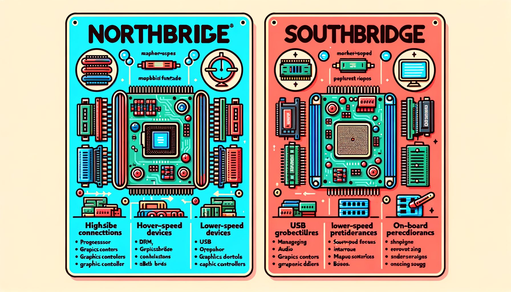
For decades, desktop and laptop motherboards followed a two-chip architecture. Sitting “north” of the system, the Northbridge connected directly to the CPU via the front-side bus (FSB). It handled the high-speed, latency-sensitive work: memory controller access (on many older designs), the graphics link (AGP in the early 2000s, later PCI Express), and sometimes cache-coherent CPU traffic. The Southbridge lived “south,” linked to the Northbridge, and took care of slower I/O: SATA/PATA storage, USB ports, onboard audio, legacy PCI slots, networking controllers, BIOS/UEFI, and real-time clock functions.
In practice, the Northbridge set the pace for memory and graphics communication with the CPU, while the Southbridge dictated port counts, controller availability, and day-to-day reliability. A motherboard’s “chipset” meant the pair working together, and it defined which features you could expect—more USB ports, RAID modes, overclocking support, or AGP/PCIe generations.
Bandwidth balance made “Northbridge vs Southbridge” a big deal. The FSB could bottleneck when memory, GPU, and CPU all fought for it. That’s why Intel’s 440BX or 975X—and later AMD chipsets—mattered to enthusiasts: they changed memory timings, bus speeds, and expansion options. In the mid-2000s, AMD charted a new course by moving the memory controller onto the CPU die (Athlon 64 era), shrinking the Northbridge’s classic role. Intel followed with integrated memory controllers starting with Nehalem. That shift set the stage for the modern design seen today, where a single controller hub plus the CPU replaces the old two-chip dance.
To visualize the old world, well, here they are—typical figures you might have seen circa 2003–2008 (values vary by platform and implementation):
| Legacy component | Typical interface | Approx. bandwidth | Role |
|---|---|---|---|
| Front-Side Bus (FSB) | Intel 800 MT/s | ~6.4 GB/s | CPU ↔ Northbridge link |
| AGP 8x | Graphics | ~2.1 GB/s | GPU ↔ Northbridge |
| PCI 32-bit/33 MHz | Expansion | ~133 MB/s (shared) | Legacy devices |
| USB 2.0 | Southbridge | 480 Mb/s per port | Peripherals |
| SATA I | Southbridge | 1.5 Gb/s per port | Storage |
The takeaway: the classic split made sense when memory controllers and graphics links needed their own high-speed hub. But once those high-speed functions moved onto the CPU, a new architecture emerged.
From two chips to one hub: CPU integration and the rise of the PCH
Starting in the late 2000s, CPU vendors began folding the Northbridge’s jobs into the processor. First went the memory controller—latency dropped significantly—then more PCI Express lanes for GPUs and NVMe SSDs followed. Intel replaced the Northbridge/Southbridge pair with a Platform Controller Hub (PCH) that carries forward the Southbridge’s I/O duties and remaining platform services. AMD took a similar path: the CPU handles memory and GPU lanes, while the chipset acts as an I/O expander.
On modern Intel desktops (e.g., 600/700-series), the CPU directly supplies PCIe lanes for the primary GPU (often PCIe 5.0 x16) and a fast M.2 NVMe slot (often PCIe 4.0 x4). The PCH contributes additional PCIe lanes, SATA ports, USB controllers, networking PHYs, and other I/O. The CPU and PCH communicate over DMI (Direct Media Interface). AMD’s AM4/AM5 platforms follow the same split: direct CPU lanes plus chipset-provided connectivity over a proprietary uplink. In laptops and many compact systems, these roles are consolidated even further into a single package or SoC—think Apple Silicon, which integrates CPU, GPU, and I/O on one die.
What’s interesting too is that the uplink between CPU and PCH has finite bandwidth. Load up multiple high-speed devices on chipset-attached lanes (e.g., extra M.2 SSDs, a 10GbE NIC, capture cards) and they ultimately share a single uplink, which can become the practical bottleneck in edge cases. Then this: CPU-attached GPU and NVMe lanes bypass the PCH entirely, giving direct, low-latency access.
Well, here it is—representative modern links and speeds you’ll encounter (varies by generation):
| Modern component | Typical interface | Approx. bandwidth (per direction) | Notes |
|---|---|---|---|
| PCIe 4.0 x4 (NVMe) | CPU or PCH | ~7.9 GB/s | Primary M.2 often CPU-attached |
| PCIe 5.0 x16 (GPU) | CPU | ~63 GB/s | High-end GPUs; some boards split lanes |
| Intel DMI 4.0 x8 | CPU ↔ PCH | Up to ~15.75 GB/s | Aggregate for chipset I/O |
| USB 3.2 Gen 2×2 | PCH | 20 Gb/s | Port speed; controller shares uplink |
| 2.5G/10G Ethernet | PCH or add-in | 2.5–10 Gb/s | Real throughput depends on uplink and PCIe lane |
In short, “Northbridge vs Southbridge” evolved into “CPU lanes vs chipset lanes.” The model is easier to reason about and usually faster overall because the CPU now handles the most latency-sensitive work. But the principle of shared bandwidth lives on in the CPU↔PCH link, so planning which devices attach where still matters for power users.
Further reading on these concepts appears in Intel’s overview of modern chipsets, AMD’s AM5 chipset pages, and summaries of Platform Controller Hub architecture. Explore high-level references at Intel’s chipset resources (https://www.intel.com/content/www/us/en/gaming/resources/chipsets.html), AMD chipsets (https://www.amd.com/en/technologies/chipsets), and the Platform Controller Hub entry (https://en.wikipedia.org/wiki/Platform_Controller_Hub).
What this means for performance, upgrades, and real-world builds
When choosing a motherboard or planning upgrades, think in terms of “CPU-attached vs chipset-attached.” Put high-performance GPUs and your fastest NVMe SSD on CPU lanes whenever possible. Additional NVMe drives, extra USB controllers, capture cards, and network adapters commonly ride on chipset lanes. Push multiple high-throughput devices on the PCH and the shared uplink can cap peak performance during heavy concurrent transfers.
Practical examples:
Gaming + streaming: Install the GPU in the primary CPU PCIe x16 slot and place your OS/game NVMe in the CPU-attached M.2. A second NVMe or a capture card may land on chipset lanes—and that’s fine, because games are mostly GPU/CPU bound. Copying large video files while streaming and capturing, however, can cause occasional dips, especially when several high-speed USB 3.2 devices hit the same controllers at once.
Content creation + AI: For 4K/8K editing or local AI inference, fast scratch disks matter a lot. Use the CPU-attached slot for the scratch NVMe if your board allows. Put archival SSDs on chipset lanes. If you rely on external SSDs (USB 3.2 Gen 2×2), remember they share the chipset uplink and may not sustain peak speeds while the system is also driving other I/O like a 10GbE NIC.
Virtualization + development: Multiple VMs performing disk-heavy tasks can saturate chipset PCIe M.2 slots when combined with network loads. Consider boards with stronger CPU lane provisioning or platforms that support PCIe bifurcation directly from the CPU (e.g., splitting x16 to multiple x4 devices), subject to CPU and board support.
Overclocking and memory: With the memory controller integrated into the CPU, memory stability depends mostly on the CPU+DIMM combo rather than a “Northbridge” limit. Chipset choice still influences features (e.g., whether memory or CPU overclocking is supported), but raw memory latency is driven by CPU architecture and DIMM specs. For best results, follow the CPU vendor’s validated memory guidelines and your board’s QVL (Qualified Vendor List).
Upgrade path and compatibility: Chipsets define how many ports you get and which standards they support (e.g., USB 4, PCIe 5.0 on storage, SATA count). CPUs define the fastest lanes and maximum memory support. If expansion is in your future—more storage, faster networking—favor boards with robust chipset lane allocation and clear documentation. Motherboard manuals usually include lane maps that show which slots share bandwidth.
Actionable steps to optimize a build:
1) Identify CPU-attached resources: Check your motherboard manual to find which PCIe slot and M.2 socket connect directly to the CPU.
2) Prioritize devices: Put the GPU and your fastest NVMe on CPU lanes. Place secondary drives and add-in controllers on chipset lanes.
3) Watch shared resources: Some boards share lanes between an M.2 slot and a PCIe slot or disable SATA ports when certain M.2 slots are populated. Plan accordingly.
4) Keep firmware and drivers fresh: Update BIOS/UEFI and chipset drivers for stability, PCIe link training improvements, and device compatibility.
5) Validate with real workloads: Run your actual tasks (game capture, batch renders, dataset ingestion) and monitor throughput. If you see contention, move devices to different slots or consider a higher-lane platform.
Helpful references include PCI-SIG for PCIe standards (https://pcisig.com/specifications), NVMe specifications (https://nvmexpress.org), and USB speed definitions (https://usb.org/defined-speed-names). These clarify what link speeds mean in practice.
Security, power efficiency, and form factor implications
With the move to CPU + PCH (or fully integrated SoCs in mobile), platform security and power management changed as well. Many systems now include firmware-based TPM (fTPM on AMD, PTT on Intel) in the CPU or chipset to meet Windows 11’s TPM 2.0 requirement. Intel’s Management Engine (ME) and AMD’s Platform Security Processor (PSP) handle low-level initialization, secure bootstrapping, and features like remote manageability in business systems. These blocks live near the PCH/SoC and sit at the heart of modern platform security models. For enterprise and prosumers, understanding them helps with compliance, encryption, and remote administration.
Power management tightened, too. I/O blocks and clock domains in the PCH can be power-gated to save energy when ports sit idle, while the CPU dynamically adjusts frequency and voltage. On laptops and mini PCs, a single-packaged SoC often integrates CPU, GPU, memory controllers, media engines, and the I/O fabric for aggressive efficiency. Apple Silicon pushes the idea further by colocating everything on one die and sharing unified memory across CPU and GPU, minimizing off-die traffic and latency. While traditional “Northbridge vs Southbridge” doesn’t apply there, the philosophy—keep latency-critical functions close and run I/O on efficient fabrics—remains the same.
Reliability considerations include thermal design and VRM quality. Packing more capability into the CPU increases heat density, and concentrating I/O into a PCH raises the stakes for good motherboard layout and cooling. For sustained high-throughput tasks, boards with heatsinked M.2 slots, adequate PCH cooling, and robust VRMs hold performance better. On workstations and servers, you’ll also see ECC memory support, wider PCIe lane counts, and sometimes separate I/O dies (as in newer AMD architectures) to balance bandwidth and thermals under heavy load.
Form factor matters. ITX boards have fewer slots and often more aggressive lane sharing, so careful planning is essential if you need multiple NVMe drives and high-speed USB simultaneously. ATX and E-ATX boards offer more headers and slots, which reduces contention. For creators and power users, picking the right form factor can be as important as the chipset choice.
For additional background on platform security engines and fabrics, see AMD’s architecture notes on chipsets (https://www.amd.com/en/technologies/chipsets) and Infinity Fabric (https://en.wikipedia.org/wiki/Infinity_Fabric), plus general references like the Northbridge and Southbridge entries (https://en.wikipedia.org/wiki/Northbridge_(computing), https://en.wikipedia.org/wiki/Southbridge_(computing)).
Q&A: common questions about Northbridge vs Southbridge today
Q: Do Northbridge and Southbridge still exist in modern PCs? A: Not in the classic two-chip sense. Their roles were largely merged into the CPU and a single Platform Controller Hub (PCH) on desktops, or a fully integrated SoC in many laptops and compact systems. Conceptually, the old Northbridge’s high-speed duties (memory, primary PCIe) moved onto the CPU, while the Southbridge’s I/O duties live in the PCH. Understanding this helps you decide which slots to use for high-performance devices.
Q: Does this change matter for gaming performance? A: Yes, but mostly behind the scenes. The CPU’s integrated memory controller reduces latency, and a GPU on CPU-attached PCIe lanes enjoys direct, fast access. For most gamers, the key is placing the GPU in the primary x16 slot and using the CPU-attached M.2 for the main NVMe SSD. Extra drives on chipset lanes rarely affect frame rates unless you’re doing heavy disk transfers while gaming.
Q: Can the chipset uplink be a bottleneck? A: In edge cases, yes. The CPU↔PCH link (e.g., DMI on Intel) has a fixed bandwidth that all chipset devices share. If you hammer multiple high-speed devices attached to the PCH—say two NVMe drives, 10GbE networking, and a 20 Gb/s USB transfer—peak throughput can be capped by that shared link. Plan critical devices on CPU lanes and stagger heavy workloads when possible.
Q: How do I find out which slot uses CPU lanes? A: Check your motherboard manual. It usually includes lane maps showing which PCIe slots and M.2 sockets connect to the CPU and which connect to the chipset. Many boards label the CPU-attached M.2 as “M2_1” or “CPU M.2,” and the top x16 slot is typically wired to the CPU. Vendor support pages and forums often provide diagrams and configuration notes.
Q: What about Apple Silicon and mobile chips—do they have Northbridge/Southbridge? A: Not as separate chips. Mobile and Apple designs integrate CPU, GPU, memory controllers, and I/O into one SoC for power efficiency and tight latency control. The underlying idea is the same—keep high-speed, latency-sensitive pathways close—but the implementation is fully integrated, which is great for battery life and thermals.
Conclusion: from two chips to smarter systems—and how to use that to your advantage
Northbridge vs Southbridge once defined how PCs worked: one chip focused on speed and memory, the other on I/O and peripherals. Today, the CPU handles the latency-critical tasks and the chipset (PCH) expands connectivity, with a single uplink between them. The shift delivers better performance, simpler designs, lower latency for memory and GPUs, and more efficient power management. For builders and upgraders, the most important concept is placement: put performance-critical devices on CPU-attached lanes and use chipset lanes for everything else.
Here’s your action plan. First, check your board’s lane map and identify which slots connect to the CPU. Second, prioritize the GPU and your fastest NVMe drive on those CPU lanes. Third, watch out for shared links and slot trade-offs—some M.2 slots disable SATA ports or reduce a PCIe slot’s width. Fourth, keep BIOS/UEFI and chipset drivers up to date for stability and performance. Finally, benchmark with your real workloads (games, renders, ingest jobs, or AI inference) and rearrange devices if you spot contention. These simple steps can yield measurable gains without extra spending.
If you’re planning a new build, choose platforms with the right mix of CPU lanes and chipset features for your needs—creators may want extra M.2 slots and high-speed USB; gamers might prioritize the cleanest x16 GPU path and a CPU-attached NVMe; home lab enthusiasts may care about bifurcation and 10GbE. Read the motherboard manual before you buy, not after, to avoid surprises and ensure every device runs at its best.
Technology names change, but the principle remains: match the fastest, most latency-sensitive devices with the fastest, most direct paths. Do that, and your system will feel snappier, stay stable under load, and scale as your projects grow. Ready to optimize your setup? Open your motherboard manual, map your lanes, and move your most important devices to CPU-attached slots today. Your future self—rendering faster, loading games quicker, or moving datasets in record time—will thank you. What part of your current build benefits most from a smarter lane layout?
Sources and further reading:
– Intel Chipset and PCH overview: https://www.intel.com/content/www/us/en/gaming/resources/chipsets.html
– AMD chipset technologies: https://www.amd.com/en/technologies/chipsets
– Platform Controller Hub (background): https://en.wikipedia.org/wiki/Platform_Controller_Hub
– Northbridge and Southbridge history: https://en.wikipedia.org/wiki/Northbridge_(computing) and https://en.wikipedia.org/wiki/Southbridge_(computing)
– PCI Express specifications: https://pcisig.com/specifications
– NVMe specifications and resources: https://nvmexpress.org
– USB speed definitions: https://usb.org/defined-speed-names
– Apple M1 SoC integration example: https://en.wikipedia.org/wiki/Apple_M1