
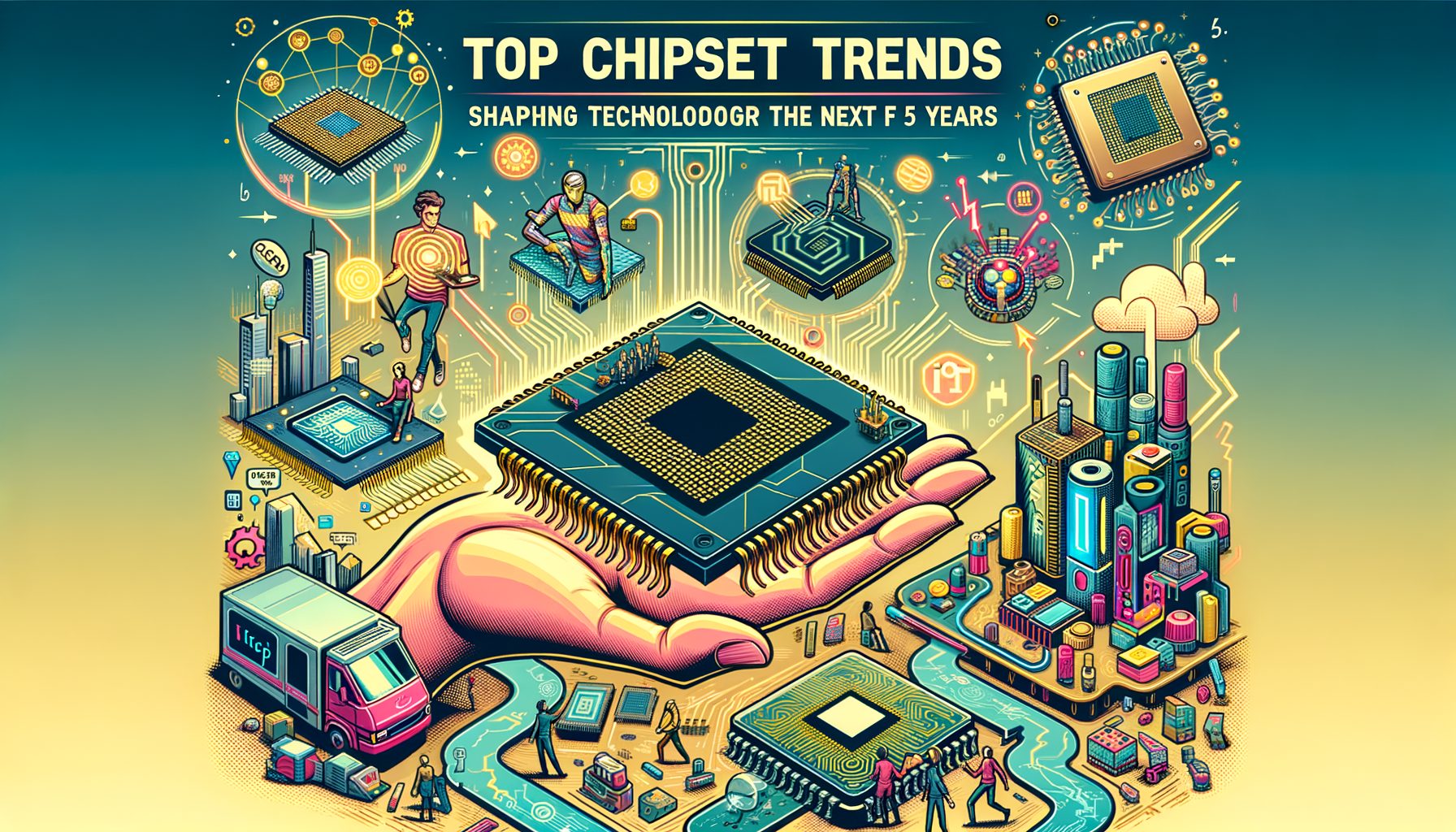
Clarity sits at the top of every builder’s worry list right now. Chip roadmaps shift quickly, AI keeps resetting performance baselines, and supply chains are being rebuilt around fresh standards. To keep a device, data center, app, or startup relevant, you need a clean read on the chipset trends that will steer tech over the next five years—and how they turn into choices you can make today.
Here’s a practical, data‑backed guide to where chip design is heading. You’ll see how chiplets and advanced packaging reshape scaling, why AI acceleration moves from cloud to every endpoint, how 2 nm and new architectures unlock efficiency, and why connectivity and security become non‑negotiable. Well, here it is: actionable steps, real examples, and credible sources you can use to plan your roadmap.
Five-Year Trend Map at a Glance
Keep this quick map handy before we dive deeper. It summarizes what is changing, when it matters, and who is driving the shift.
| Trend | Milestones (2025–2030) | Why It Matters | Key Standards / Players |
|---|---|---|---|
| Chiplets & Advanced Packaging | UCIe 2.0 adoption; 2.5D/3D stacking mainstream; HBM3E capacity surge | Faster time-to-market, mix-and-match IP, huge memory bandwidth | UCIe, TSMC CoWoS/SoIC, Intel Foveros, Samsung I-Cube |
| AI Acceleration Everywhere | Cloud GPUs scale; on-device NPUs hit 40+ TOPS for consumer PCs | Lower latency, privacy by default, cost control for inference | MLCommons, Microsoft Copilot+ PC baseline |
| 2 nm & New Architectures | 2 nm/GAA mass production ramps; backside power; RISC-V expands | More perf/W, smaller form factors, domain-specific efficiency | TSMC N2, Intel 18A/PowerVia, Samsung SF2, RISC‑V International |
| Connectivity & Security by Design | 5G‑Advanced (Rel‑18), Wi‑Fi 7 certs; confidential computing spreads; PQC pilots | Trust at scale, faster links, future‑proof cryptography | 3GPP Rel‑18, Wi‑Fi Alliance, NIST PQC |
The Chiplet Era and Advanced Packaging Become the Default
Monolithic scaling—cramming more transistors onto a giant die—hits physical, cost, and yield walls. The next five years will be dominated by chiplets: small dies, each tuned for a function (CPU, GPU, NPU, IO, cache), linked by high‑speed die‑to‑die fabrics and advanced packaging. Yields improve, process nodes can be mixed (bleeding‑edge logic, mature IO), and time‑to‑market shortens because not every block needs a full re‑spin.
Standardization is the critical enabler. Universal Chiplet Interconnect Express (UCIe) aims to do for chiplets what PCIe did for expansion cards: interoperable, vendor‑agnostic connectivity. With UCIe 2.0 (2024), features for streaming and new use cases broadened, and the ecosystem now spans major foundries, IP providers, and hyperscalers. Expect catalogs of third‑party chiplets to “snap” into custom SoCs—especially for AI and networking—much like cloud builders assemble white‑box servers. For a detailed spec overview, see the UCIe consortium’s site at ucie.org.
Advanced packaging turns modular theory into practical performance. 2.5D interposers and 3D stacking pull compute and memory closer, slashing latency while boosting bandwidth. HBM sits at the center. With HBM3E, vendors report per‑stack bandwidth in the terabytes per second, allowing AI models to run faster and cut energy per token by feeding accelerators at adequate rates. Micron documents HBM3E performance in its technical notes (micron.com).
Then this: if you’re a system designer, plan for a chiplet‑ready future. Prioritize UCIe in your roadmaps and evaluate packaging partners (TSMC CoWoS/SoIC, Intel Foveros, Samsung I‑Cube). If you’re a software founder, assume AI accelerators and memory hierarchies will diversify; design runtimes that schedule across heterogeneous compute and memory pools. If you buy hardware, seek products with transparent chiplet roadmaps—openness usually signals lower lock‑in risk and better long‑term optimization.
Bottom line: chiplets and advanced packaging convert the physics of small distances into a strategic edge. Winners will treat package design, memory topology, and interconnects as first‑class architecture decisions, not last‑minute integration chores.
AI Acceleration From Cloud to Edge: NPUs Go Mainstream
AI is no longer a single “GPU in a rack” story. Acceleration will distribute: giant clusters for training and batch inference, plus NPUs in PCs, phones, cars, and cameras for low‑latency, privacy‑preserving tasks. Evidence already shows up in industry benchmarks like MLPerf from MLCommons, where rapid, iterative gains appear across training and inference as vendors co‑design silicon, compilers, and quantization to lower cost per inference. Browse the latest results at mlcommons.org to track throughput and energy efficiency by workload.
On the consumer side, Microsoft’s Copilot+ PC criteria draw a clear line: a local NPU with 40+ TOPS for features like on‑device summarization or image generation. That baseline pushes app developers to target NPUs first, with fallbacks to GPU or CPU. For privacy‑focused or regulated environments, the impact is direct: sensitive data stays local while still enabling smart assistants and multimodal features.
What’s interesting too: in the data center, memory bandwidth and interconnects define real‑world performance more than raw FLOPs. HBM3E, NVLink‑class GPU‑to‑GPU fabrics, and Ethernet/InfiniBand with congestion control and collectives will make or break scaling. Expect more domain‑specific accelerators (speech, recommendation, vector databases) and runtimes that pick the right silicon for each stage. Also watch mixed‑precision compute (FP8/INT4) and sparsity—both now central to boosting throughput without blowing power budgets.
Practical steps if you build AI products: design your inference stack to detect and target NPUs automatically (via ONNX Runtime, TVM, or vendor SDKs). Make quantization‑aware training routine in your ML workflow. Budget for bandwidth; when a model is memory‑bound, moving to HBM‑backed instances can beat brute‑force GPU counts. If you’re a device maker, document NPU ops, memory limits, and supported frameworks clearly—developers dislike guesswork, and clarity attracts the best apps.
One more factor: energy. The International Energy Agency estimates data centers’ electricity consumption could reach 620–1,050 TWh by 2026, up from roughly 460 TWh in 2022, driven in part by AI demand. See the IEA’s 2024 analysis at iea.org. Silicon that trims joules per inference gains a compounding advantage across scale, sustainability targets, and cost of goods sold.
New Process Nodes and Architectures: 2 nm, GAA, RISC‑V, and Heterogeneous Computing
Process technology still matters, but the narrative has shifted from “smaller is always better” to “pick the right node, with the right architecture, in the right place.” Two transitions define the next half decade: gate‑all‑around (GAA) transistors at 2 nm‑class nodes and greater architectural diversity—from x86 and Arm to rapidly expanding RISC‑V deployments.
Aggressive roadmaps have been detailed by leading foundries. TSMC’s N3 is in high‑volume production, and N2 (2 nm‑class) is planned to ramp in 2025. With Intel’s 18A and backside power delivery (PowerVia), IR drop is reduced and frequency headroom can rise by separating power and signal layers. Samsung has announced a 2 nm timeline for mobile first, then HPC. These shifts aren’t only about density; perf/W improves and form factors shrink, rippling into longer battery life and denser AI accelerators. Explore official roadmaps at tsmc.com, intel.com, and semiconductor.samsung.com.
Architecture tells the other half of the story. Arm‑based designs rule mobile and are expanding in laptops and servers. RISC‑V, an open instruction set, grows quickly in microcontrollers, AI accelerators, and custom SoCs because designers can add domain‑specific instructions and avoid licensing constraints. RISC‑V International tracks ecosystem growth and tools at riscv.org. Meanwhile, x86 vendors double down on heterogeneous designs—combining performance and efficiency cores, integrated NPUs, and fast media engines to balance power and responsiveness.
What should teams do about it? Treat heterogeneity as the baseline. Plan for “DSP here, NPU there, CPU orchestrating” rather than one giant general‑purpose core. Embrace compilers and runtimes that span architectures (LLVM/MLIR, oneDNN, cuDNN, CoreML, SNPE, TVM). For procurement, evaluate total platform maturity: toolchains, driver stability, and long‑term security updates often outweigh a small benchmark delta. And if you build your own silicon, ask early how packaging, interconnect, and memory choices will amplify—or bottleneck—a shiny new node; no one wants 2 nm compute starving behind last‑generation IO.
The meta‑trend is co‑design: hardware, system software, model architecture, and packaging optimized together. Products will feel faster, cooler, and longer‑lasting than spec sheets imply when those roadmaps align.
Efficiency, Security, and Connectivity: The New Non‑Negotiables
Performance is table stakes; the differentiators over the next five years will be energy efficiency, security by design, and reliable high‑speed connectivity. These aren’t “nice to have” features. They anchor compliance, user trust, and total cost of ownership.
Efficiency: Every watt counts. Expect aggressive use of dynamic voltage and frequency scaling, power gating, near‑threshold operation for background tasks, and workload‑aware scheduling across CPU/GPU/NPU. Memory is the silent energy eater; designs that keep data close (HBM, stacked SRAM, better caching) will win, especially for AI inference and analytics. Energy metrics—like joules per token for LLMs—are set to become as common as latency or accuracy.
Security: Confidential computing, memory safety, and post‑quantum readiness will spread from the cloud into endpoints. Server silicon now ships with hardware‑based trusted execution environments (e.g., Intel TDX, AMD SEV‑SNP) to isolate workloads. On devices, hardware memory tagging (such as Arm MTE) helps eliminate whole classes of memory bugs. Regulators increasingly require cryptographic agility, and while quantum threats aren’t immediate for consumers, planning must start. NIST’s post‑quantum process has drafted standards for key encapsulation and signatures (e.g., Kyber, Dilithium); begin evaluating hardware acceleration paths and migration strategies now. References: NIST PQC and Arm MTE.
Connectivity: 5G‑Advanced (3GPP Release 18) brings enhanced uplink, positioning, and AI‑native network features that matter for XR, industrial IoT, and connected vehicles. Wi‑Fi 7 certification from the Wi‑Fi Alliance enables wider channels and multi‑link operation, cutting latency and improving stability in congested environments. Chipsets tuned for these standards will unlock smoother real‑time collaboration, streaming, and edge offload. Overviews live at 3gpp.org and wi-fi.org.
Next steps: if you run infrastructure, tie silicon selection to your energy and security KPIs. Choose platforms with mature TEEs, hardware roots of trust, and clear patch lifecycles. For product managers, align features with connectivity realities—no point promising near‑instant cloud features to users behind congested links without local NPU fallbacks. For startups, “secure by default and efficient by design” becomes a selling point customers will pay for.
Quick Q&A
Q: Are chiplets only for big companies?
A: No. As UCIe matures and packaging services expand, mid‑size teams can integrate third‑party chiplets instead of designing every block. Think of it like using proven IP libraries—just at the package level.
Q: Will on‑device NPUs replace cloud AI?
A: Not entirely. Expect a hybrid: local NPUs for private, low‑latency tasks; cloud clusters for heavy training and large‑scale analytics. Good products will switch between them seamlessly.
Q: Is 2 nm mainly marketing?
A: The name is partly branding, yet underlying changes (GAA, backside power, new materials) deliver real perf/W gains. Value depends on how well memory and software integrate with the silicon.
Q: How urgent is post‑quantum cryptography for me?
A: If you store data that must remain secure for years, start planning now—“harvest now, decrypt later” is a real concern. Use NIST’s guidance and pilot migrations where feasible.
Q: What should I measure beyond TOPS or FLOPs?
A: Track end‑to‑end latency, energy per task (e.g., joules per inference), memory bandwidth utilization, and software portability. Those better reflect real experience and cost.
Conclusion
Across chiplets, AI acceleration, 2 nm‑class nodes, and stronger connectivity and security, one theme stays constant: integration beats isolated specs. Chiplets and advanced packaging let you compose exactly the silicon you need. AI moves fluidly across cloud and device, so software must target heterogeneous compute. New process technologies and architectures improve efficiency, but they only pay off when memory, interconnect, and compilers keep pace. Users no longer accept trade‑offs on security or responsiveness; chipset choices now shape trust and experience directly.
If you are a founder, architect, or buyer, act on three steps this quarter: (1) Map workloads to a hybrid AI plan—decide what must run locally on NPUs and what belongs in the cloud. (2) Engage vendors about UCIe and packaging roadmaps; ask how they will mix nodes and memory to hit your latency and energy targets. (3) Align with security and sustainability goals early—select platforms with confidential computing, a clear patch strategy, and measurable energy efficiency. Then this: treat them as product‑market fit enablers, not side quests.
The next five years will reward teams who co‑design hardware and software, embrace open standards, and measure what matters in the user journey. Start small if you need to—prototype an NPU‑first feature, audit data‑center energy per inference, or evaluate a chiplet‑enabled SKU—but start now. Momentum compounds.
Your roadmap is a lever. Pull it with intention. What is one workload in your stack you could make faster, cheaper, and more private by matching it to the right silicon this month?
Sources
Universal Chiplet Interconnect Express (UCIe) Consortium
International Energy Agency: Data Centres and Data Transmission Networks
Intel Foundry Technology (Including PowerVia/18A)
NIST Post‑Quantum Cryptography Project