
Chipset technology sits inside almost everything with a power button, yet many buyers still find the history and spec sheets confusing. Clarity is the real hurdle: marketing buzzwords often blur the factors that decide speed, battery life, heat, and AI capability. In the pages ahead, you’ll see how chipset design evolved—from early discrete logic to modern AI-centric systems—so you can buy with confidence. By the end, you will understand how chipsets work, why they matter, and how to pick the right one for your needs in 2025 and beyond.
From Discrete Logic to SoCs: The First Big Leap (1970s–2000s)
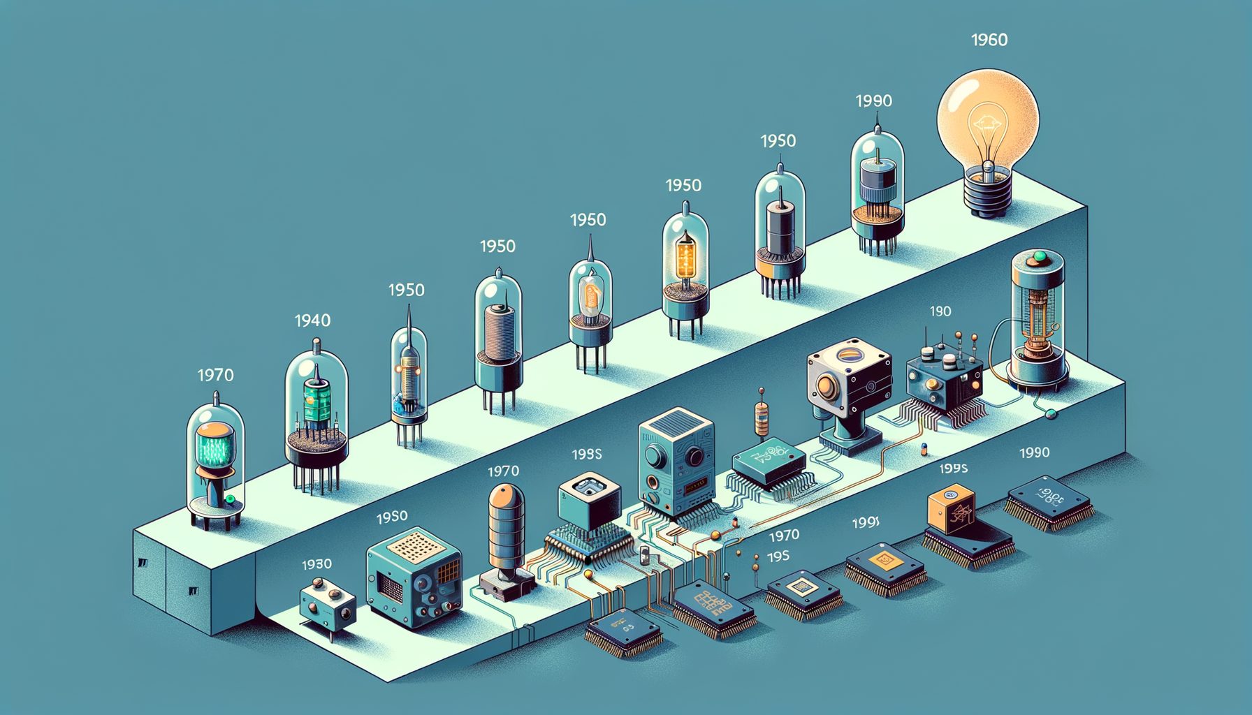
During the 1970s, computing shifted from boards packed with many small chips to integrated microprocessors—single dies able to execute instructions and manage basic tasks. Milestones such as the Intel 4004 and 8086 kicked off the age of general-purpose CPUs, yet many companion chips were still required for memory, graphics, and I/O. Through the 1980s and 1990s, the typical PC relied on two support hubs—the northbridge for memory and graphics traffic and the southbridge for I/O—forming the “chipset” around the CPU. That architecture dominated desktops and servers for years, but downsides persisted: extra board space, higher power draw, and added latency between key components.
By the late 1990s and early 2000s, integration took center stage. Rather than parking the memory controller off-chip, designers placed it inside the CPU. AMD made this mainstream in the early 2000s, slicing memory latency and boosting real-world performance in games and databases. Meanwhile, semiconductor processes shrank from micrometers to nanometers, jamming more transistors into the same area and lifting both speed and efficiency. Then came the opening for the next phase: the system-on-chip (SoC).
SoCs consolidated multiple functions—CPU, GPU, memory controllers, and more—onto a single piece of silicon. The gains were concrete: faster internal communication, lower power, and reduced cost and footprint. Early wins showed up in embedded gear and media devices. What’s interesting too, the mobile boom became the inflection point. As phones added internet, navigation, and advanced cameras, engineers learned to prize efficiency without sacrificing responsiveness. By the mid-2000s, chipset design wasn’t just about clock speed; it was about smart integration, thermal control, and distributing work across specialized blocks like graphics and signal processors. That pivot laid the groundwork for the smartphone era.
Mobile Revolution and Power Efficiency: How Smartphones Forced a Rethink (2007–2016)
Smartphones flipped the priority stack. Performance per watt—not maximum peak—ruled the day. Battery life, heat, and sustained throughput mattered more than brief benchmark bursts. The iPhone era accelerated custom silicon and fierce competition. ARM-based designs led with energy-savvy instruction sets and power management. Techniques such as big.LITTLE paired high-performance cores with efficient cores, switching between them to conserve energy during light tasks while keeping headroom for gaming, imaging, or browsing.
In this period, modems, GPUs, image signal processors, and secure enclaves joined the CPU on the same die. The chipset became the traffic cop for everything: 4G, Wi‑Fi, HDR photography, and even early AR. As nodes moved from 45 nm to 28 nm and then 16/14 nm, better thermals and thinner phones followed. Camera upgrades—multi-frame noise reduction, real-time face detection—were increasingly handled by dedicated accelerators inside the SoC, cutting latency and saving power versus running them on general-purpose cores.
Manufacturers also embraced the idea of sustained performance. A chip that blazes for seconds only to throttle is less useful than one that stays brisk for minutes. Hence the rise of careful thermal design, power gating to shut down idle units, and fine-grained voltage scaling. Integrating the modem trimmed power during network use, which matters for streaming and navigation. In short, specialization beat brute force. Chipsets evolved into coordinated teams—CPUs, GPUs, signal engines, and security blocks—each optimized for its lane.
AI, Chiplets, and 3D Packaging: The Modern Era of Chipset Innovation (2017–Today)
Starting around 2017, artificial intelligence moved from the data center into pockets and backpacks. NPUs—neural processing units and similar accelerators—were added to run matrix math and neural networks efficiently. On-device AI delivered practical wins: faster photo tweaks, voice features without the cloud, instant translation, and better privacy because data stays local. Metrics expanded, too; buyers now see TOPS (tera operations per second) and, increasingly, TOPS per watt alongside CPU and GPU numbers. Heterogeneous computing took hold as different blocks ran parts of a workload in parallel for speed and efficiency.
Packaging innovation kept pace. Instead of one giant monolithic die, designers embraced chiplets—multiple smaller dies linked at high speed inside a single package. That approach improves yield, reduces cost, and allows mixing technologies (say, advanced compute tiles with more mature I/O tiles). 3D stacking and through-silicon vias brought memory like HBM closer to compute, boosting bandwidth while controlling power. Intel’s Foveros 3D packaging, AMD’s chiplet strategies, and UCIe standards hint at a future built from interoperable “Lego blocks” of silicon. Meanwhile, EUV lithography enabled dense 7 nm, 5 nm, and 3 nm nodes, with 2 nm and nanosheet transistors on deck, further raising the performance-per-watt bar.
Well, here it is: a compact table of milestones to anchor those shifts. The numbers are rounded but capture the arc of integration and efficiency.
| Year | Notable Chipset | Approx. Process | Approx. Transistors | Key Breakthrough |
|---|---|---|---|---|
| 1971 | Intel 4004 | 10 µm | ~2,300 | First commercial microprocessor |
| 2003 | AMD Athlon 64 | 130 nm | ~100M | Integrated memory controller |
| 2013 | Apple A7 | 28 nm | ~1B | Early 64-bit mobile SoC |
| 2020 | Apple M1 | 5 nm | ~16B | High perf/watt laptop-class SoC |
| 2022–2023 | HPC/AI GPUs (e.g., H100) | 4N/5 nm class | ~80B+ | AI acceleration, HBM stacking |
NPUs, chiplets, and advanced packaging now define the modern chipset. Then this: longer phone battery life, faster laptop content creation, and massive AI training and inference at scale. For consumers, the practical tip is simple—don’t stop at CPU cores and clocks. Check AI acceleration, memory bandwidth, and thermal headroom, especially if you’ll run on-device AI, edit video, or game on the go.
Practical Guide: Choosing the Right Chipset in 2025
Shopping in 2025 means reading past the buzzwords. Start with your main workload. For smartphones used mostly for messaging, streaming, and browsing, an efficient midrange SoC with a strong modem and reliable camera pipeline can beat a throttling flagship. Look for NPUs that support your preferred AI apps; more on-device AI brings lower latency and better privacy. If video capture matters, prioritize image signal processing—multi-frame HDR and efficient 4K/8K encode—so you don’t overheat.
Laptops live and die by performance per watt and sustained thermals. Thin-and-light machines should pair integrated GPUs with capable NPUs so everyday AI features—summarization, transcription, image generation—run smoothly without fan noise. Memory bandwidth and storage speed influence everything from app launches to creative timelines, so verify both. For photo and video work, a balanced chip with strong media engines and an NPU for AI assist may outshine a CPU-heavy setup. Gamers can weigh discrete GPUs, but also check CPU cache, boost behavior, and whether the cooling system can hold clocks under load. Battery-first buyers should look at process-node efficiency (newer generally helps), claimed all-day life, and independent tests of sustained performance.
Edge devices and small form-factor PCs bring connectivity into focus. Seek Wi‑Fi 6E or Wi‑Fi 7, fast storage links, and security features such as hardware enclaves and modern virtualization support. Across every category, software longevity is decisive. A stellar chipset without long-term drivers or security patches ages fast. Also, judge the AI story honestly: TOPS isn’t everything—framework support, memory capacity, and thermals matter. An NPU that sustains a solid fraction of its rated TOPS for minutes, not seconds, will feel faster in real life.
As a quick checklist: match the chipset to your workload; confirm sustained performance in third-party reviews; ensure the NPU and GPU fit your creative or AI tasks; verify connectivity and storage; and favor devices with proven update histories. Follow that, and you won’t get lost in spec sheets.
FAQs
Q: What is a chipset in modern devices? A: It’s the core silicon platform that includes the CPU plus supporting blocks like GPU, NPU, memory controllers, modems, and security hardware. In phones and many laptops, this arrives as a system-on-chip that integrates most functions into one die or package.
Q: Do more CPU cores always mean better performance? A: Not always. Many tasks benefit more from stronger single-core speed, better GPU or NPU acceleration, or higher memory bandwidth. Balanced design and sustained thermals often beat raw core counts.
Q: What does the “nanometer” number really mean? A: It’s shorthand for a manufacturing generation. Smaller often correlates with better efficiency and density, but numbers aren’t directly comparable across foundries. Lean on real-world tests and power measurements.
Q: Why do NPUs matter now? A: On-device AI jobs—image enhancement, transcription, local assistants—run faster and more efficiently on NPUs than on general CPUs. Responsiveness improves, privacy benefits, and battery life holds up.
Q: How can I keep my device from overheating? A: Don’t block vents, keep software updated, limit heavy multitasking in hot environments, and choose devices with proven cooling. For phones, game modes that cap frame rates can cut heat.
Conclusion
Chipset design has moved from scattered components orbiting a CPU to tightly integrated systems that orchestrate CPUs, GPUs, NPUs, modems, and security engines in one efficient package. We traced the journey from early microprocessors and PC-era northbridge/southbridge boards, through the smartphone-driven push for efficiency, to today’s AI acceleration, chiplets, and advanced packaging. The throughline is better performance per watt: more capability, less energy, lower latency. For buyers, the best device isn’t the one with the biggest peak number; it’s the one that sustains performance, manages heat, and supports the features you actually use—especially on-device AI.
Your next move: list your top three tasks—gaming, content creation, communications, or AI-assisted workflows—and map them to the chipset traits that matter most: sustained CPU/GPU speed, NPU capability, memory bandwidth, and thermal design. Then cross-check with independent reviews under sustained load. If stuck between two devices, favor stronger software support and a proven update record; the device will feel “new” longer. Power users should validate compatibility with AI frameworks and media codecs; everyone else can focus on battery life under typical use, not synthetic peaks.
The future looks bright. As 3 nm and 2 nm nodes mature—and chiplet ecosystems and 3D stacking expand—we’ll see leaps in capability without losing efficiency. Open standards and better packaging will let designers mix the best blocks for each job, while on-device AI quietly upgrades photos, calls, and creative work. If this guide cleared the spec-sheet fog, share it with a friend who’s shopping soon and bookmark the links for deeper dives. What matters most to you—battery life, silent operation, or AI responsiveness? Your answer will point you to the right chipset and the right device. Keep learning, stay curious, and make the silicon work for you.
Helpful Outbound Links
Intel 4004 history | ARM big.LITTLE overview | TSMC EUV technology | Apple M1 announcement | AMD chiplet architecture explained | UCIe (Universal Chiplet Interconnect Express) | IEEE Spectrum on AI chips
Sources
Intel Museum: The Story of the Intel 4004; ARM: big.LITTLE Technology; TSMC: EUV Overview; Apple Newsroom: M1 Announcement; AMD Community: Chiplet Architecture Explained; IEEE Spectrum: AI Chips Coverage; Vendor technical briefs and public product pages from 2013–2025 for process, packaging, and NPU trends.