
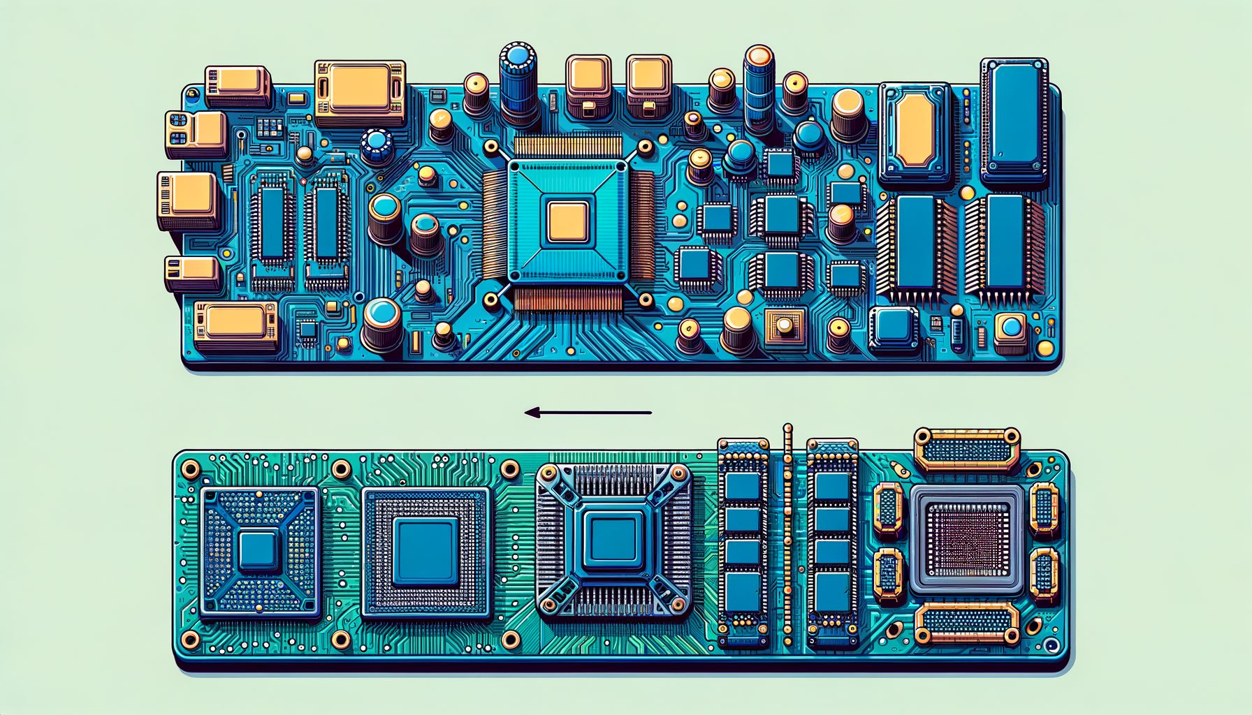
The semiconductor world is hitting a wall: AI workloads are exploding, battery life still matters, costs are rising, and time-to-market is brutal. That’s where modular chipsets step in. In simple terms, “modular chipsets” break a system-on-chip (SoC) into smaller pieces—often called chiplets—then stitch them back together with ultra-fast links. The promise is big: better yields, faster product refreshes, lower cost per function, and custom mixes of CPU, GPU, NPU, memory, and analog blocks. Curious about how SoC design is evolving, why chiplets dominate the headlines, and whether they’ll shape your phone, laptop, car, or data center? This guide lays it out clearly.
From Monolithic SoCs to Modular Chipsets: What Changed and Why Now?
For decades, chipmakers improved performance by cramming more transistors into a single, monolithic die. That strategy still works—up to a point. Physics and economics now push against it. The reticle limit for a single die is roughly 850–860 mm², which constrains how big a single chip can be. As dies get larger, yield drops because a single defect can spoil the whole device. Meanwhile, moving to bleeding-edge nodes can cost tens or even hundreds of millions in non-recurring engineering (NRE) and mask sets. AI also changed the game: modern models need vast parallel compute, fat memory bandwidth, and specialized accelerators, which don’t always fit neatly into a one-size-fits-all die.
Modular chipsets address these constraints by splitting functionality into smaller dies—compute cores, graphics, AI accelerators, I/O, RF/analog, or memory—fabricated on the best process for each function, then integrated in a package. Such a “right-node-for-the-right-IP” approach lets designers use advanced nodes for logic while keeping analog or I/O on mature, cheaper nodes. AMD popularized the approach in desktop and server CPUs with chiplet-based EPYC and Ryzen lines, improving yields and letting the company mix core counts efficiently. Intel’s Foveros and EMIB packaging stack or bridge dies to build multi-die processors, and Nvidia’s latest GPUs increasingly pair with high-bandwidth memory (HBM) through advanced packaging. What’s interesting too: even consumer products like high-end Macs combine multiple dies via ultra-dense links, hinting at the mainstream future.
Crucially, the timing is right because die-to-die interconnects and packaging have matured. Ultra-short reach links can move data at tens of gigatransfers per second per lane with sub-nanosecond-class latencies, narrowing the performance gap between on-die and in-package communication. Standards like UCIe (Universal Chiplet Interconnect Express) aim to make multi-vendor chiplets interoperable, while foundries like TSMC, Intel, and Samsung now offer robust 2.5D and 3D stacking services at scale. In short, modular is no longer a lab curiosity—it’s becoming a production reality.
The Business Case: Cost, Yield, and Speed via Chiplets and 3D Packaging
Why do so many roadmaps now point to modular chipsets? Economics. Yield is boosted when a huge SoC is split into smaller dies because each die faces fewer defects on average. Better yield means lower cost per good part. Chiplets can also be developed and validated in parallel by different teams, proven blocks can be reused across product generations, and features like core count can scale by adding more compute chiplets without a full SoC redesign. The result: shorter time-to-market and far more SKU flexibility.
Another driver is mask cost and NRE. Advanced nodes carry eye-watering mask prices; reusing established chiplets avoids paying that bill for every new variation. Companies can keep certain functions (like analog, DDR/PCIe PHYs, or RF) on mature nodes that are cheaper, reliable, and have higher voltage tolerance, while moving AI or CPU tiles to leading-edge nodes. Packaging becomes the new “system integration point,” shifting value from a single giant die to a carefully orchestrated multi-die assembly.
There are trade-offs: packaging yield matters, testing must ensure “known good die,” and die-to-die links consume power and add latency versus on-die wires. But for many products—especially servers, AI accelerators, and high-end PCs—the savings and flexibility outweigh the overhead. Even in mobile and automotive, modular approaches can help segment features across trims, lean into local supply chains, and offer mid-cycle refreshes by swapping a die rather than spinning a full SoC.
| Factor | Monolithic SoC | Modular/Chiplet SoC | Notes |
|---|---|---|---|
| Yield on large designs | Lower as die size grows | Higher (smaller dies) | Chiplets reduce scrap from single defects |
| Mask/NRE cost per variant | High, repeated per SKU | Amortized via reuse | Advanced node masks can exceed $20M |
| Time-to-market | Long (full-chip re-spin) | Shorter (parallel development) | Mix-and-match chiplets for fast SKUs |
| Performance scaling | Limited by reticle, power | Scales via more tiles | AI, cores, memory tiles expand bandwidth/compute |
| Power/latency overhead | Lowest (on-die) | Higher (die-to-die) | Mitigated by short, dense links and 3D |
Packaging technologies make this all viable. Then this: 2.5D interposers (e.g., TSMC CoWoS) place logic dies beside HBM for terabyte-per-second bandwidth, while bridges (Intel EMIB) and 3D stacking (Intel Foveros, TSMC SoIC) reduce distance further. When combined with standards like UCIe, the outcome is a modular platform strategy that lets companies ship more targeted products with fewer full redesigns and better return on engineering investment.
Useful links: TSMC’s 3DFabric overview explains CoWoS and SoIC options (TSMC 3DFabric), and SemiEngineering regularly tracks mask cost escalation and yield economics (SemiEngineering).
The Tech Stack: Interconnects, AI Accelerators, and Memory Options That Make Modularity Work
Modular chipsets depend on three pillars: high-density packaging, fast die-to-die interconnects, and a software stack that treats many dies like one system. On the physical side, silicon interposers and advanced bridges allow thousands of short wires between chiplets, supporting massive bandwidth at low energy per bit. For example, the UCIe standard targets up to tens of gigatransfers per second per lane, with energy below a picojoule per bit and latencies low enough to host memory semantics across dies. Vendor technologies—AMD’s Infinity Fabric, Intel’s EMIB and Foveros—deliver similar outcomes with proprietary tuning, and they’re already in shipping products.
Memory is the other half of the performance story. HBM3 and HBM3E stacks deliver bandwidth well above 800 GB/s per stack, and systems can place multiple stacks adjacent to compute tiles using 2.5D packaging. That proximity shortens the path to memory, dramatically improving performance per watt versus off-package DRAM. On the client side, LPDDR5X and GDDR6 offer flexible options, while embedded SRAM/Cache chiplets or 3D-stacked SRAM can serve ultra-low-latency needs when paired closely with CPU/GPU/NPU tiles.
Compute heterogeneity is where modular shines. You can pair general-purpose CPU cores (Arm, x86, or RISC-V) with fixed-function NPUs or matrix engines optimized for transformer inference. A product aimed at the edge might combine a modest CPU tile, a strong NPU tile, and a connectivity/RF tile made on an older node. A data-center accelerator might combine many compute tiles with HBM and a control tile, then scale to multi-tile modules. Software bridges the complexity: drivers, runtime schedulers, and compilers distribute work across tiles, while security enclaves and roots of trust protect keys and firmware.
Interoperability is improving. The UCIe Consortium pushes a common PHY and protocol mapping so chiplets from different vendors could one day plug-and-play. Foundries and OSATs are building standardized flows for “known good die,” design-for-test (DfT), and thermal simulation. And open ecosystems—RISC-V in particular (RISC-V International)—enable more teams to design specialized tiles without license constraints that traditionally slowed experimentation.
Roadblocks and How Industry Is Solving Them: Latency, Power, Thermals, Security, and Software
Modularity isn’t magic. The biggest technical trade-offs are latency and power overheads from leaving the monolithic die. On-die wires are incredibly efficient; any bump across dies adds serialization/deserialization, clocking, and equalization costs. Engineers fight this by keeping links as short and wide as possible, adopting ultra-short-reach PHYs, using advanced interposers or 3D stacking to minimize distance, and placing latency-sensitive functions (like caches) on the same tile. Active interposers and backside power delivery can further cut congestion and improve energy per bit.
Thermals are another challenge. When multiple hot chiplets sit close together—especially in 3D stacks—heat density and hotspots complicate cooling. Solutions include thermal vias, die-thinning, improved heat spreaders, liquid cooling for high-end modules, and smarter power management at the tile level. Yield at the package level may also drop if even one die in a multi-die assembly fails; “known good die” testing, robust binning, and redundancy schemes mitigate this risk. Over time, packaging yields tend to improve as volumes rise and processes mature, echoing what happened in earlier semiconductor transitions.
Verification and software complexity can’t be ignored. More boundaries mean more protocols, corner cases, and failure modes. To manage this, teams adopt comprehensive DfT, boundary scan, link margining, and system-level emulation. On the software side, unified memory models, standardized driver stacks, and AI/ML frameworks that target heterogeneous accelerators are key. The goal is to present a single logical system to developers while maximizing the strengths of each tile underneath.
Security extends from silicon to software. Chiplets must authenticate each other, boot paths must be measured and verified, and data in motion across die-to-die links should be protected. Hardware roots of trust, secure enclaves, and signed firmware are becoming table stakes. Open efforts like OpenTitan show how transparent designs can strengthen trust, while industry leaders integrate secure boot and isolation at the tile and package levels.
Finally, the ecosystem must align. Standards such as UCIe, plus packaging options from foundries and OSATs, help avoid lock-in and spread costs across many customers. Intel details EMIB and Foveros for bridge-and-stack designs (Intel Advanced Packaging), while TSMC’s CoWoS and SoIC play in similar spaces. As interoperability, toolchains, and supply chains mature, many of today’s barriers are trending downward—making modular chipsets increasingly practical across segments, not just in flagship servers.
Q&A: Quick Answers to Common Questions
Is a modular chipset the same as a chiplet design? Almost. “Modular chipset” is a broad idea of building systems from swappable blocks; “chiplet” usually means those blocks are individual silicon dies integrated in one package. Many modular chipsets are chiplet-based, but the concept also includes 3D-stacked or bridged dies and even discrete co-processors.
Will modular chipsets make devices upgradeable like PCs? Not typically for phones. Packaging is dense and custom, so consumer-level upgrades are rare. However, OEMs can refresh products faster by swapping or scaling tiles, and modular desktop/server platforms already benefit from flexible SKUs.
Do chiplets hurt performance? They can add some latency and power overhead, but advanced interposers, bridges, and 3D stacking minimize it. For many workloads—especially parallel AI/graphics—more compute tiles plus close HBM outweigh the overhead, improving overall performance-per-watt.
How do small teams get started? Consider mature nodes for analog/I-O, evaluate UCIe-ready IP, partner with a foundry/OSAT for 2.5D/3D packaging, and use open ecosystems (e.g., RISC-V). Leverage EDA flows that support multi-die verification and DfT for known good die.
Conclusion: Modular Is a Mindset—And It’s Reshaping the Roadmap
We began with a real problem: monolithic scaling is harder, AI-hungry workloads won’t wait, and costs keep climbing. Modular chipsets—most visibly through chiplets—offer a practical path forward. By distributing functions across specialized dies, companies improve yield, reuse proven IP, shorten development cycles, and tailor products to exact needs. The hardware stack is ready: 2.5D interposers, 3D stacking, and high-speed die-to-die interconnects (UCIe, EMIB, Foveros, Infinity Fabric) are shipping now. The memory story is strong too, with HBM and advanced DRAM options feeding compute-hungry cores and NPUs. Yes, challenges remain—latency/power overheads, thermals, verification, and security—but industry solutions are maturing fast, and standards are converging.
If you’re building products, act now. Start a modular feasibility checklist: Which IP must live on advanced nodes, and which can stay on mature nodes? What’s your die partitioning strategy and test plan for known good die? Are you evaluating UCIe-capable PHYs and packaging partners that fit your volumes and thermals? Can your software stack abstract multiple tiles as one coherent system? These steps translate the promise of modularity into predictable schedules, lower risk, and targeted performance-per-watt gains.
Developers and tech enthusiasts should also watch the signals: growing mentions of “chiplets,” “HBM,” and “3D packaging” in product briefs often forecast big jumps in AI performance and efficiency. Expect more devices—from laptops to edge servers—to tout modular architectures, not as buzzwords, but as concrete reasons for better battery life, cooler operation, and smarter AI on-device.
Now is the best time to get informed, build internal champions, and pilot a modular design, even on a small scale. Well, here it is: bookmark this guide, share it with your team, and pick one next action this week—evaluate a die-to-die IP block, talk to a packaging partner, or map your SoC into candidate chiplets. The future favors teams that learn fast and design flexibly. Are you ready to modularize your roadmap and turn constraints into your next competitive edge?
Sources and further reading:
– UCIe Consortium: Universal Chiplet Interconnect Express overview and specifications — https://www.ucie.org
– TSMC 3DFabric: CoWoS, InFO, and SoIC advanced packaging — https://www.tsmc.com/english/dedicatedFoundry/technology/3DFabric
– Intel Advanced Packaging (EMIB, Foveros) — https://www.intel.com/…/advanced-packaging/overview.html
– AMD multi-chip module and Infinity Fabric background — https://www.amd.com/en/technologies/infinity-architecture
– SemiEngineering: Economics of advanced nodes, yields, and mask costs — https://semiengineering.com
– RISC-V International: Open ISA ecosystem — https://riscv.org
– OpenTitan: Open-source silicon root of trust — https://opentitan.org/